Surface acoustic wave element and surface acoustic wave device using the same

a surface acoustic wave and element technology, applied in piezoelectric/electrostrictive/magnetostrictive devices, semiconductor devices, piezoelectric/electrostriction/magnetostriction machines, etc., can solve the problem of increasing the stock amount, and affecting the performance of the device. the effect of reducing the element swing and good oscillation property

Inactive Publication Date: 2009-01-06
SEIKO EPSON CORP
View PDF9 Cites 1 Cited by
  • Summary
  • Abstract
  • Description
  • Claims
  • Application Information

AI Technical Summary

Benefits of technology

[0014]An advantage of the invention is to provide a surface acoustic wave element and surface acoustic wave device at a low price, having a good oscillation property, which can be used in applications for various electronic devices.
[0015]According to a first aspect of the invention, a surface acoustic wave element includes a piezoelectric substrate, an IDT composed of a pair of first and second comb-like electrodes, formed around a center of the piezoelectric substrate, and formed on a surface of the surface acoustic wave element, and a pair of first and second terminals electrically connected to the IDT, formed at central and peripheral areas of the piezoelectric substrate, respectively, in which a package is bonded with an adhesive to a surface of the surface acoustic wave element, opposite to the surface formed with the IDT.
[0016]According to this aspect of the invention, the pair of first and second terminals is formed at the central and peripheral areas of the piezoelectric substrate respectively. Therefore, in the case of using this surface acoustic wave element in applications for a mobile electric device, the central area is coated with the adhesive to reduce a swing of the element in association with moving while the pair of terminals formed at this central area is wire-boded. In the case of use in applications for a hardly mobile electric device, the peripheral area is coated with the adhesive to reduce an influence on an oscillation property in association with a contraction stress of the adhesive while the pair of terminals formed at the peripheral area is wire-bonded. Therefore, this one type of SAW element can deal with both the mobile and immobile electronic devices.
[0017]Thus, a surface acoustic wave element at a low price, having a good oscillation property can be provided, which can be used in applications for various electronic devices.
[0018]In the above-mentioned structure, it is preferable that the pair of terminals be disposed at one side of the piezoelectric substrate in a latitudinal direction.
[0019]In this manner, since the pair of terminals is disposed at one side of the piezoelectric substrate in a latitudinal direction, in the case of the surface acoustic wave element connected to the semiconductor element through a bonding wire, the bonding wire can be shortened by disposing the aforementioned side where the pair of terminal is formed, at a side where the semiconductor element is disposed.

Problems solved by technology

In the SAW device 1 having the central area of the aforementioned piezoelectric element 4 bonded to the package 2, however, there is a fear of a change in an oscillation property due to warpage in the area formed with the IDT 5, which is resulted from contraction stress of the adhesive 3 or the like.
In consideration of both cases where the SAW device is used in applications for mobile electronic devices such as a cellar telephone and used in applications for hardly mobile electronic devices, it is necessary to prepare two types of SAW devices 1, 9 different in positions of the terminals 7, 7, resulting in relatively expensive design development costs as well as causing increase in a stock amount.

Method used


Image

  • Surface acoustic wave element and surface acoustic wave device using the same
  • Surface acoustic wave element and surface acoustic wave device using the same
  • Surface acoustic wave element and surface acoustic wave device using the same

Examples


Embodiment Construction

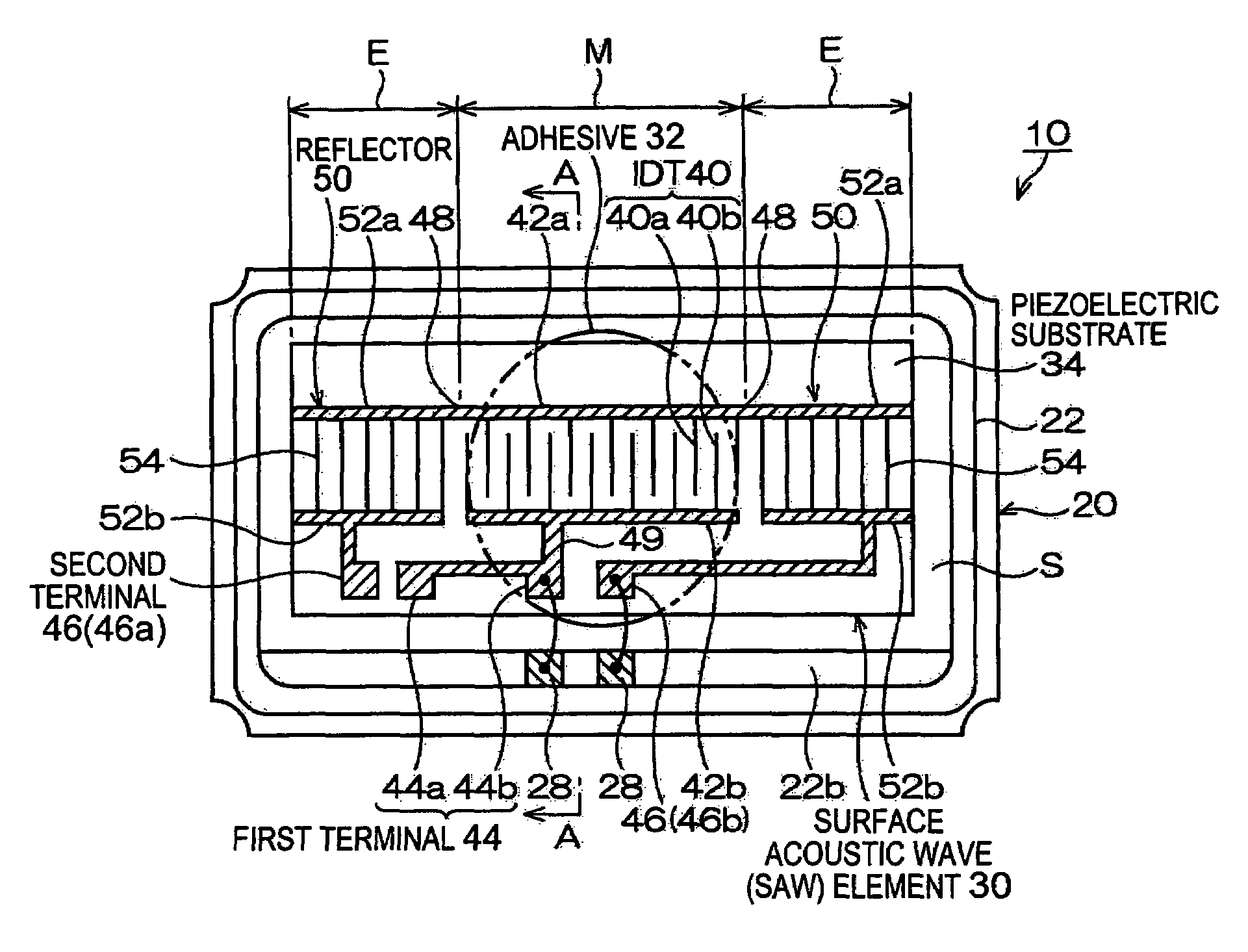
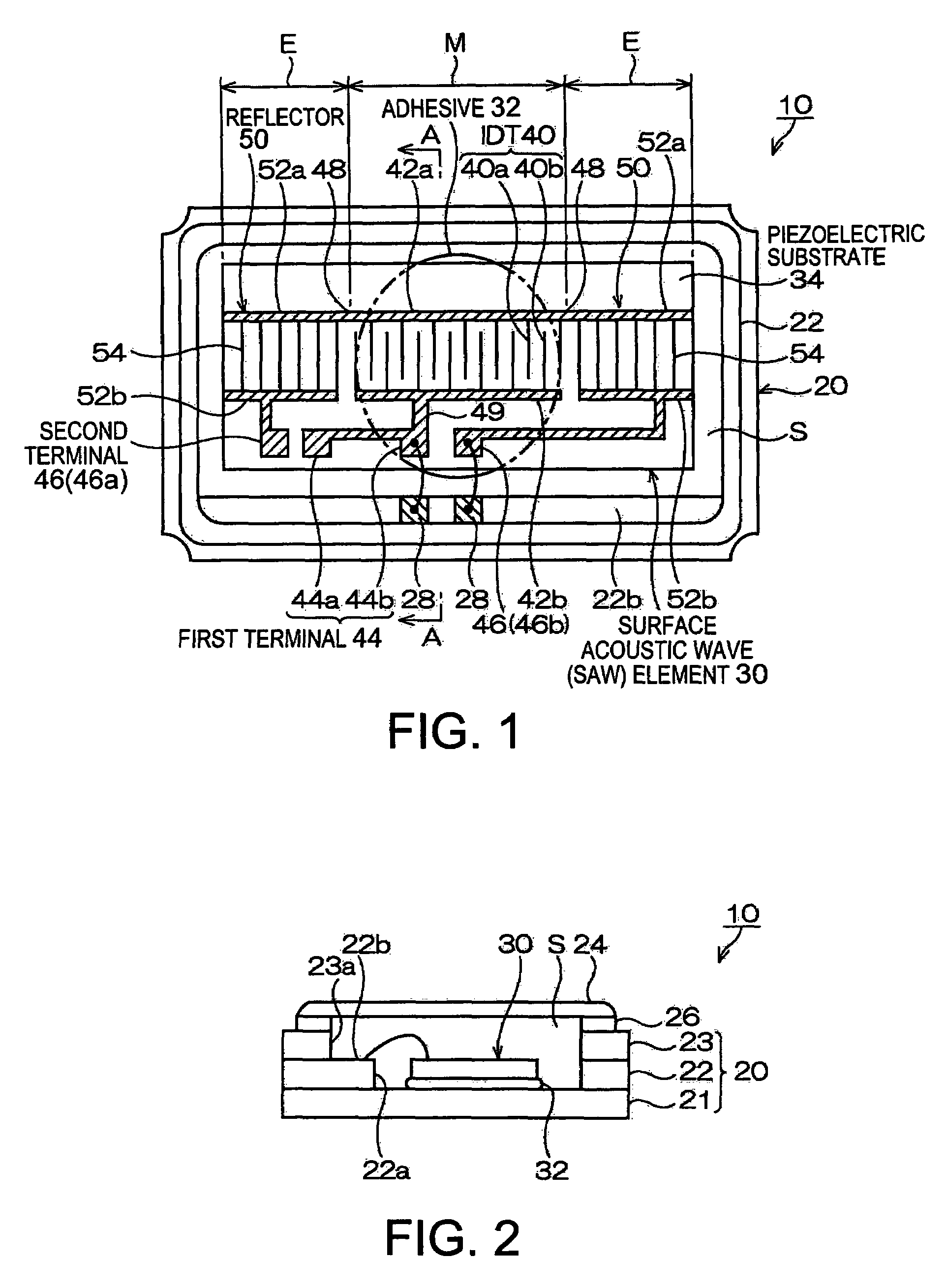
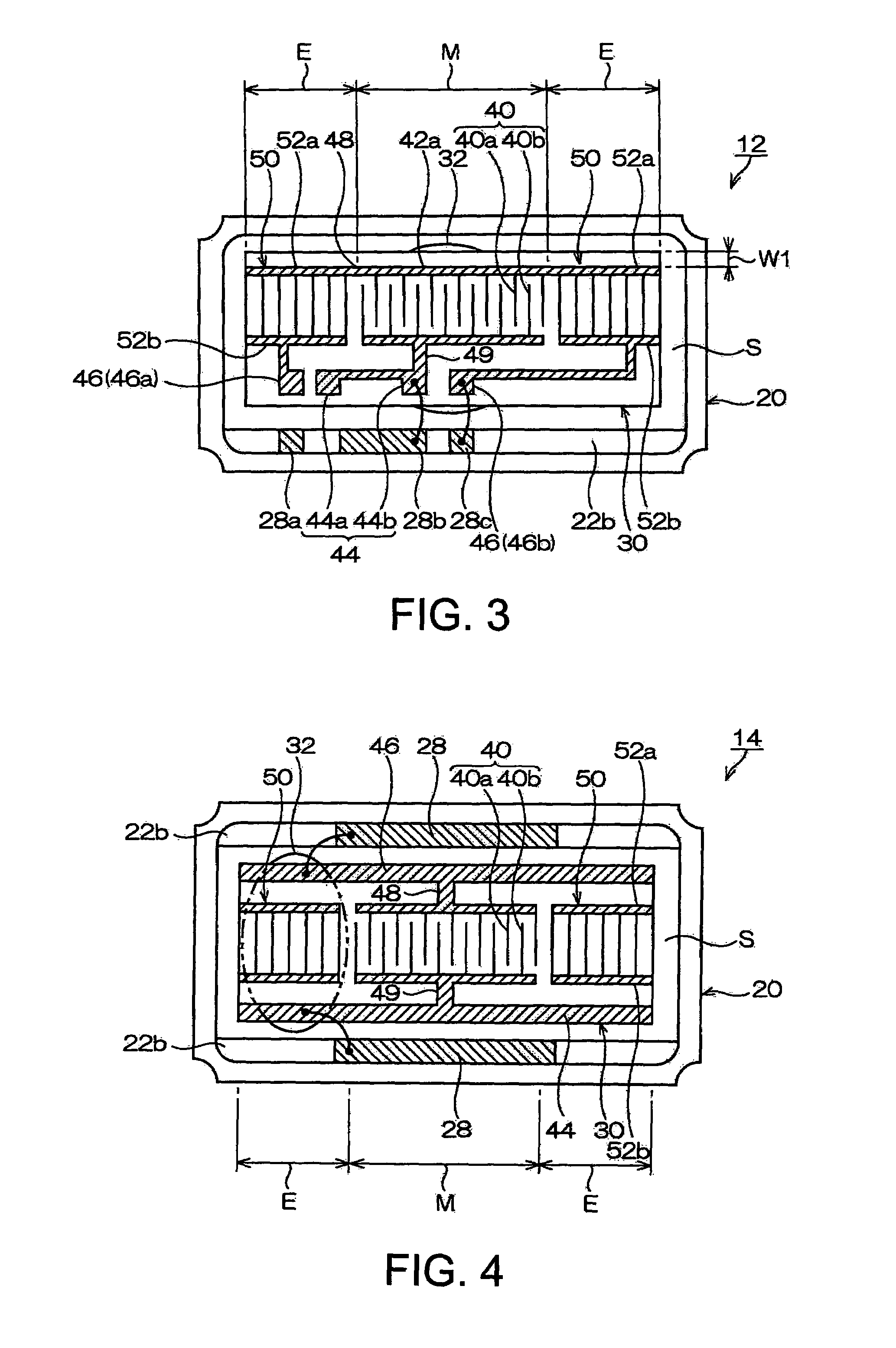
[0035]FIGS. 1 and 2 show a surface acoustic wave device (hereinafter referred to as a “SAW device”) 10 according to an embodiment of the invention, in which FIG. 1 shows a schematic plain view of the surface acoustic wave device and FIG. 2 shows a schematic cross section view of FIG. 1 along the line A-A. Meanwhile, FIG. 1 shows a view that is seen through a casing for convenience of understanding. Parallel oblique lines in FIG. 1 do not express a cross section.

[0036]In those FIGS., the SAW device 10 contains an electronic surface wave element (hereinafter referred to as a “SAW element”) 30 in a package 20.

[0037]As shown in FIG. 2, the package 20 is wholly formed in a substantially rectangular shape by a sintering after lamination of first, second, and third substrates 21, 22, 23 as an insulating material, which are formed by shaping a ceramic green sheet of oxidized aluminum.

[0038]The second and third substrates 22, 23 each have predetermined via holes 22a, 23a inside such that an ...


PUM


Abstract

A surface acoustic wave element includes a piezoelectric substrate, an IDT composed of a pair of first and second comb-like electrodes, formed around a center of the piezoelectric substrate, and formed on a surface of the surface acoustic wave element, and a pair of first and second terminals electrically connected to the IDT, formed at central and peripheral areas of the piezoelectric substrate, respectively, in which a package is bonded with an adhesive to a surface of the surface acoustic wave element, opposite to the surface formed with the IDT.

Description

BACKGROUND OF THE INVENTION[0001]1. Technical Field[0002]The present invention relates to a surface acoustic wave element and a surface acoustic wave device using the same.[0003]2. Related Art[0004]A surface acoustic wave device (hereinafter referred to as a “SAW device”) is widely used in applications for compact information equipments such as HDDs (Hard Disk Drives), mobile computers, or IC cards, or mobile communication equipments such as cellar telephones, automobile telephones, or paging systems.[0005]FIG. 6 is a schematic perspective view of an existing SAW device 1, in which a piezoelectric element 4 is contained in a package.[0006]An IDT (Inter Digital Transducer) composed of a pair of comb-like electrodes 5a, 5b is formed around a center of the piezoelectric element 4, and reflectors 6, 6 are formed at opposite sides of the IDT 5, respectively.[0007]The piezoelectric element 4 is bonded to an inner bottom of the package 2 using an adhesive 3 in a manner to bond a central ar...

Claims


Application Information

Patent Timeline
Patent Type & Authority Patents(United States)
IPC IPC(8): H03H9/25
CPCH03H9/0585H03H9/1071H01L2224/32225H01L2224/45144H01L2224/48091H01L2224/48227H01L2224/73265H01L2924/16195H01L2924/00014H01L2924/00
Inventor SHINDO, TAKEHIKO
Owner SEIKO EPSON CORP
Why Eureka
Try Eureka