Method of growing carbon nanotubes and method of manufacturing field emission device using the same

a carbon nanotube and field emission technology, which is applied in the manufacture of cold cathode, electric discharge tube/lamp, electric discharge system, etc., can solve the problems of difficult manufacturing of large-scale field emission devices, difficult to use glass substrates in in situ processes, and damage to thin films formed on substrates such as gate electrode insulating layers, etc., to achieve superior field emission characteristics and low cost

Inactive Publication Date: 2009-01-20
SAMSUNG SDI CO LTD
View PDF0 Cites 62 Cited by
  • Summary
  • Abstract
  • Description
  • Claims
  • Application Information

AI Technical Summary

Benefits of technology

[0010]The present invention provides a method of growing carbon nanotubes at a low temperature. The present invention also provides a method of growing carbon nanotubes that is able to control the density of the carbon nanotubes. The present invention also provides a method of growing carbon nanotubes at low costs. The present invention also provides a method of manufacturing a field emission device, which can prevent damages of thin films such as a gate electrode insulating film during a thermal process. The present invention also provides an inexpensive method of manufacturing a large size field emission device by growing carbon nanotubes at a low temperature, and provides a method of manufacturing a field emission device having superior field emission characteristics by controlling the density of carbon nanotubes of the emitter.

Problems solved by technology

Typical glass such as sodalime glass, however, softens at temperature of approximately 480° C. Therefore, it is difficult to use the glass substrate in an in situ process which requires temperature greater than 500° C. for growing the carbon nanotubes.
Even though a high temperature glass is used as a substrate material, thin films formed on the substrate such as a gate electrode insulating layer can be peeled off or damaged due to thermal stresses generated between thin films or between a thin film and the substrate, because temperature greater than 500° C. is applied to the glass substrate to grow carbon nanotubes by an in situ process.
Therefore, it is difficult to manufacture a commercial large size field emission device using the thermal CVD method due to above mentioned or other reasons.

Method used


Image

  • Method of growing carbon nanotubes and method of manufacturing field emission device using the same
  • Method of growing carbon nanotubes and method of manufacturing field emission device using the same
  • Method of growing carbon nanotubes and method of manufacturing field emission device using the same

Examples


Embodiment Construction

[0026]The present invention will now be described in more detail with reference to the accompanying drawings in which exemplary embodiments of the invention are shown.

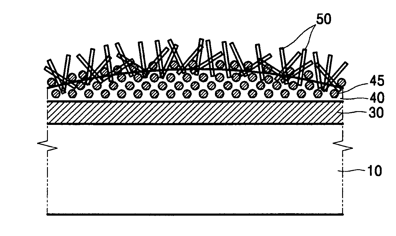
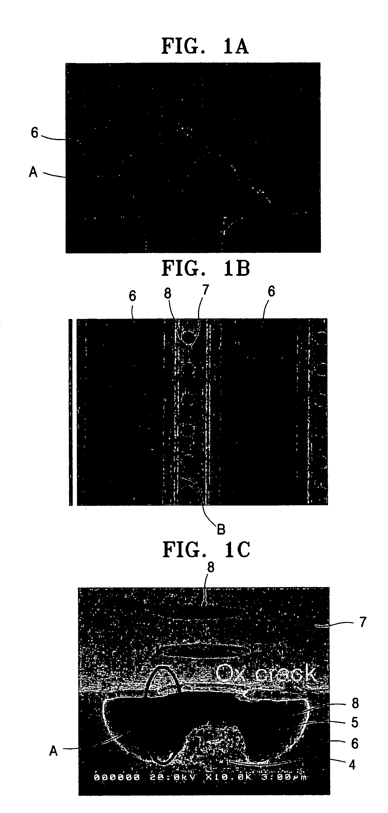
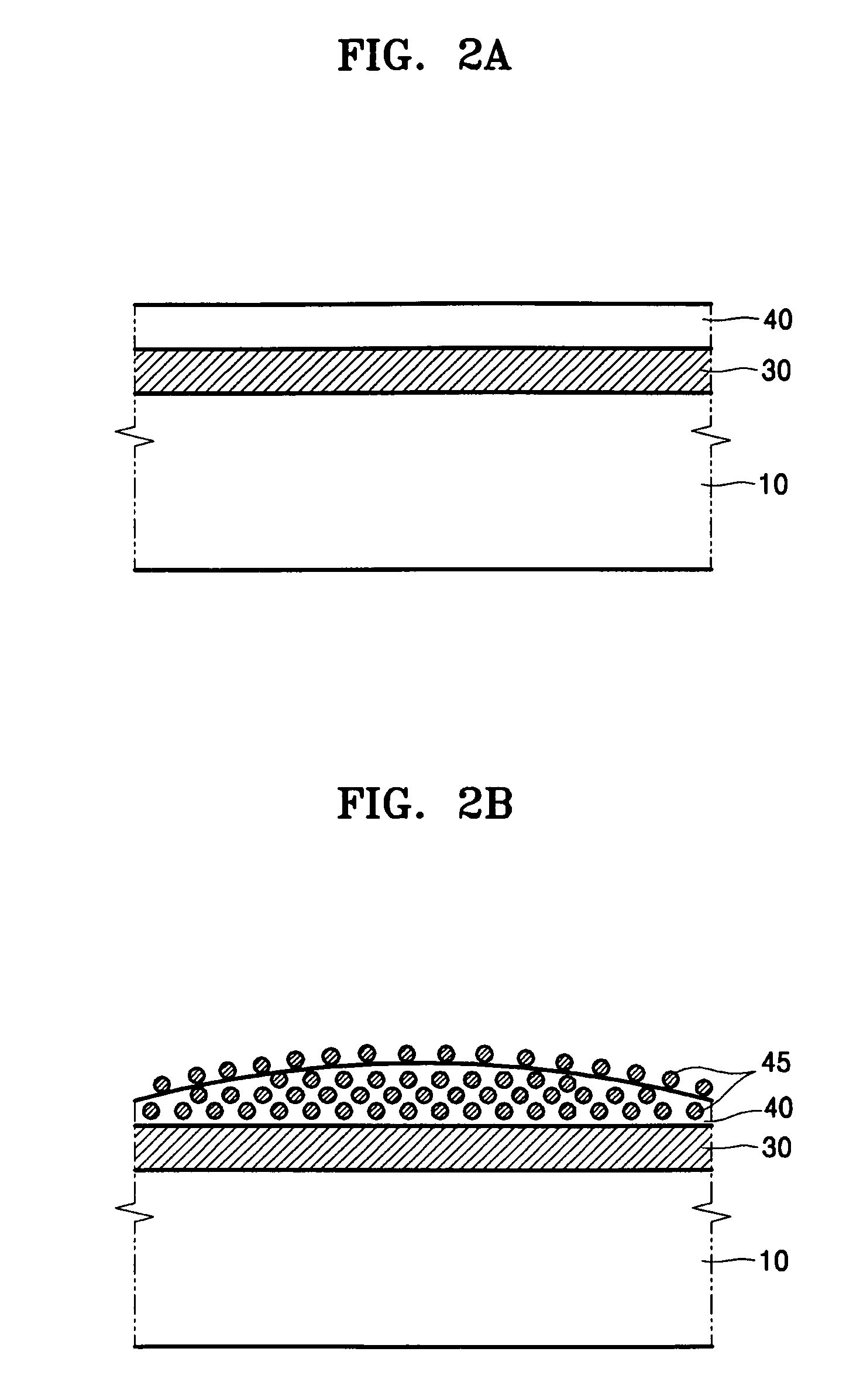
[0027]FIG. 1A is a plan view of a dummy region of a field emission device having a carbon nanotube emitter formed using a CVD method. FIG. 1B is a plan view of a display region of the field emission device of FIG. 1A, and FIG. 1C is a scanning electron microscope (SEM) image of a cross-sectional view of a display region of the field emission device of FIG. 1A.

[0028]As depicted in FIG. 1A, when carbon nanotubes are grown on a catalyst metal layer (not shown) of a substrate (not shown) using an in situ process of a CVD method, crack A is generated in gate electrode insulating film 6 formed between the substrate and a gate electrode (not shown). Also, in this case, as depicted in FIG. 1B, crack A formed in gate electrode insulating film 6 extends to gate electrode 7, and causes another crack B in gate electrode 7 around w...


PUM

PropertyMeasurementUnit
temperatureaaaaaaaaaa

Abstract

Methods of growing carbon nanotubes and manufacturing a field emission device using the carbon nanotubes are provided. The method of growing carbon nanotubes includes the steps of preparing a substrate, forming a catalyst metal layer on the substrate to promote the growing of the carbon nanotubes, forming an amorphous carbon layer on the catalyst metal layer where the amorphous carbon layer partially covers the catalyst metal layer, and growing the carbon nanotubes from a surface of the catalyst metal layer. The carbon nanotubes are grown in a portion of the surface of the catalyst metal layer that is not covered by the amorphous carbon layer. In the method of growing carbon nanotubes, the carbon nanotubes are grow at a low temperature. A density of carbon nanotubes can be controlled to improve field emission characteristics of an emitter of a field emission device.

Description

CLAIM OF PRIORITY[0001]This application makes reference to, incorporates the same herein, and claims all benefits accruing under 35 U.S.C. § 119 from an application for METHOD FOR GROWING CARBON NANOTUBES AND MANUFACTURING METHOD OF FIELD EMISSION DEVICE THEREWITH, earlier filed in the Korean Intellectual Property Office on Dec. 13, 2005 and there duly assigned Serial No. 10-2005-0122426.BACKGROUND OF THE INVENTION[0002]1. Field of the Invention[0003]The present invention relates to a method of growing carbon nanotubes and a method of manufacturing a field emission device using the same, and more particularly, to an inexpensive method of growing carbon nanotubes, where the carbon nanotubes can be grown at a low temperature with a suitable density for an emitter of a field emission device, and an inexpensive method of manufacturing a field emission device using the same, in which the field emission device can be constructed to have superior electron emission characteristics, and dama...

Claims


Application Information

Patent Timeline
Patent Type & Authority Patents(United States)
IPC IPC(8): H01J9/00C23C16/00D01F9/12
CPCB82Y30/00B82Y40/00C01B31/0233H01J1/304H01J9/025H01J2201/30469Y10S977/876C01B32/162
Inventor KIM, HA-JINHAN, IN-TAEK
Owner SAMSUNG SDI CO LTD
Why Eureka
Try Eureka