Power supply step-down circuit and semiconductor device

a power supply and step-down circuit technology, applied in the direction of electric variable regulation, process and machine control, instruments, etc., can solve the problems of inability to step down the input power supply voltage, low voltages that may be applied to the lsi circuit, and extremely small size of semiconductor integrated circuits (lsi circuits) within the semiconductor device, so as to maintain the reliability and serviceable life of the lsi circuit, and reduce resistance. , the effect of increasing the reaction speed

Inactive Publication Date: 2009-01-20
FUJITSU SEMICON LTD
View PDF9 Cites 2 Cited by
  • Summary
  • Abstract
  • Description
  • Claims
  • Application Information

AI Technical Summary

Benefits of technology

[0021]Another and more specific object of the present invention is to provide a power supply step-down circuit and a semiconductor device, which can maintain the reliability and the serviceable life of the LSI circuit, even with respect to the LSI circuit provided with a single power supply step-down circuit that integrally has the step-down circuit for the normal operation mode and the step-down circuit for the standby mode.
[0022]Still another object of the present invention is to provide a power supply step-down circuit adapted to a semiconductor integrated circuit having a first operation mode and a second operation mode having a smaller current consumption than the first operation mode, comprising a first step-down circuit, activated only during the first operation mode, and configured to step down an input power supply voltage to an output voltage; a second step-down circuit, provided integrally with the first step-down circuit and activated only during the second operation mode, and configured to step down the input power supply voltage to an output voltage; an output terminal configured to output the output voltage of one of the first and second step-down circuits that is activated, the first step-down circuit having a lower resistance, higher reaction speed and a larger current consumption compared to the second step-down circuit; and an output circuit configured to maintain the output voltage that is output from the output terminal lower than the input power supply voltage for a first predetermined time when an operation mode makes a transition from the first operation mode to the second operation mode, so that the output voltage that is output from the output terminal does not become the same potential as the input power supply voltage for a second predetermined time or longer. According to the power supply step-down circuit of the present invention, it is possible to maintain the reliability and the serviceable life of the semiconductor integrated circuit, even with respect to the semiconductor integrated circuit provided with a single power supply step-down circuit that integrally has the step-down circuit for the normal operation mode and the step-down circuit for the standby mode.
[0024]A further object of the present invention is to provide a semiconductor device comprising the power supply step-down circuit described immediately above, and a circuit part configured to receive the output voltage that is output from the output terminal and includes a CPU and / or a logic circuit. According to the semiconductor device of the present invention, it is possible to maintain the reliability and the serviceable life of the semiconductor integrated circuit, even with respect to the semiconductor integrated circuit provided with a single power supply step-down circuit that integrally has the step-down circuit for the normal operation mode and the step-down circuit for the standby mode.

Problems solved by technology

Due to improvements made in the semiconductor producing processes that form extremely small patterns, the size of semiconductor integrated circuits (LSI circuits) within the semiconductor device has become extremely small, and voltages that may be applied to the LSI circuits have become low.
For this reason, in the standby mode, it is not possible to step down the input power supply voltage using the power supply step-down circuit having the relatively large current consumption on the order of several hundred μA to several mA, for example.
But when the step-down circuit for the normal operation mode and the step-down circuit for the standby mode are provided separately within the LSI circuit, there is a limit to reducing the area occupied by the step-down circuit part as a whole.
Furthermore, because the differential amplifier 4 has a high resistance, the current consumption of this circuit part becomes small.
But since the current consumption of the LSI circuit in the standby mode is small, it takes time for the output voltage to drop to the original or proper potential.
For this reason, there were problems in such a case that the reliability of the LSI circuit will deteriorate, and the serviceable life of the LSI circuit will be shortened.

Method used


Image

  • Power supply step-down circuit and semiconductor device
  • Power supply step-down circuit and semiconductor device
  • Power supply step-down circuit and semiconductor device

Examples


Embodiment Construction

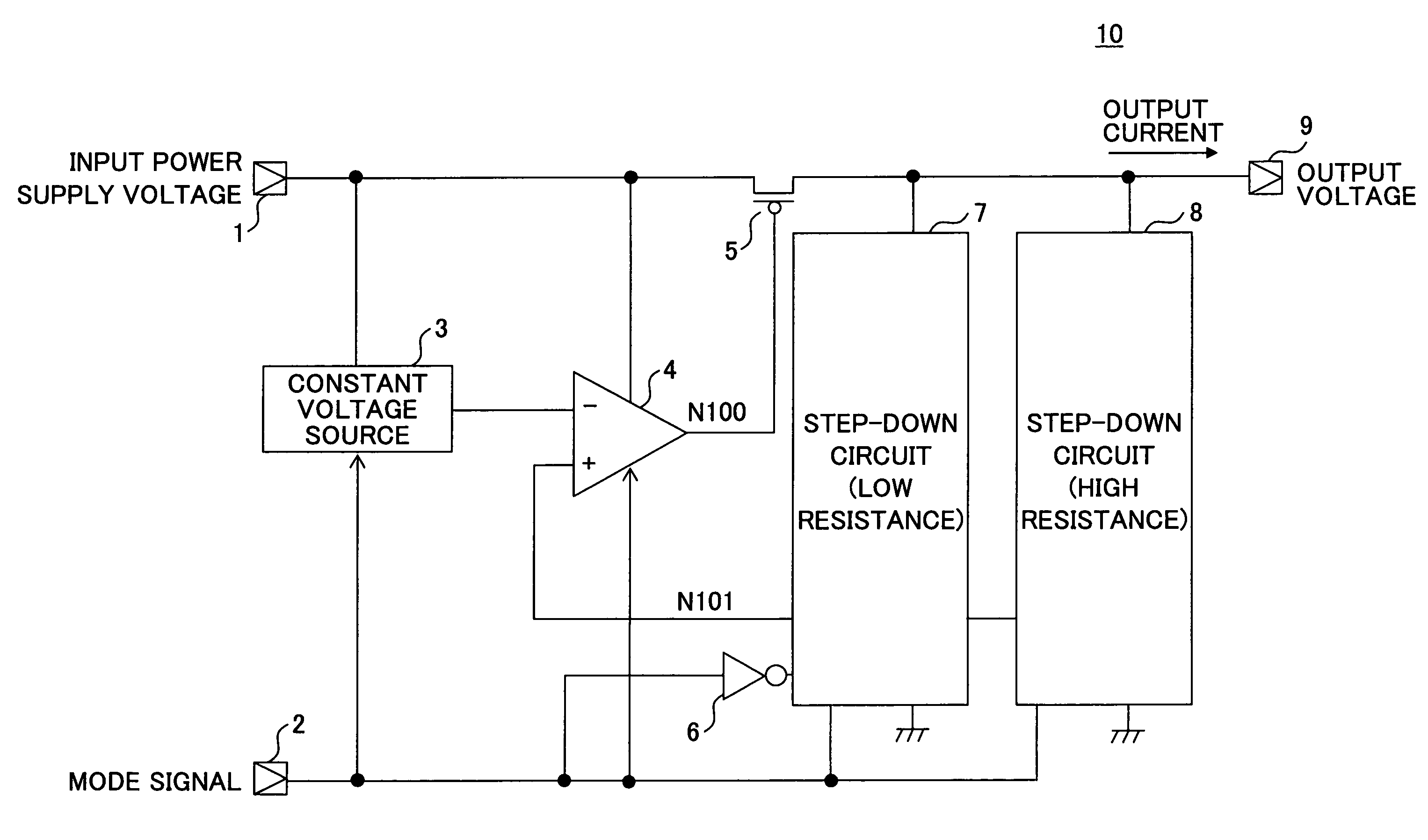
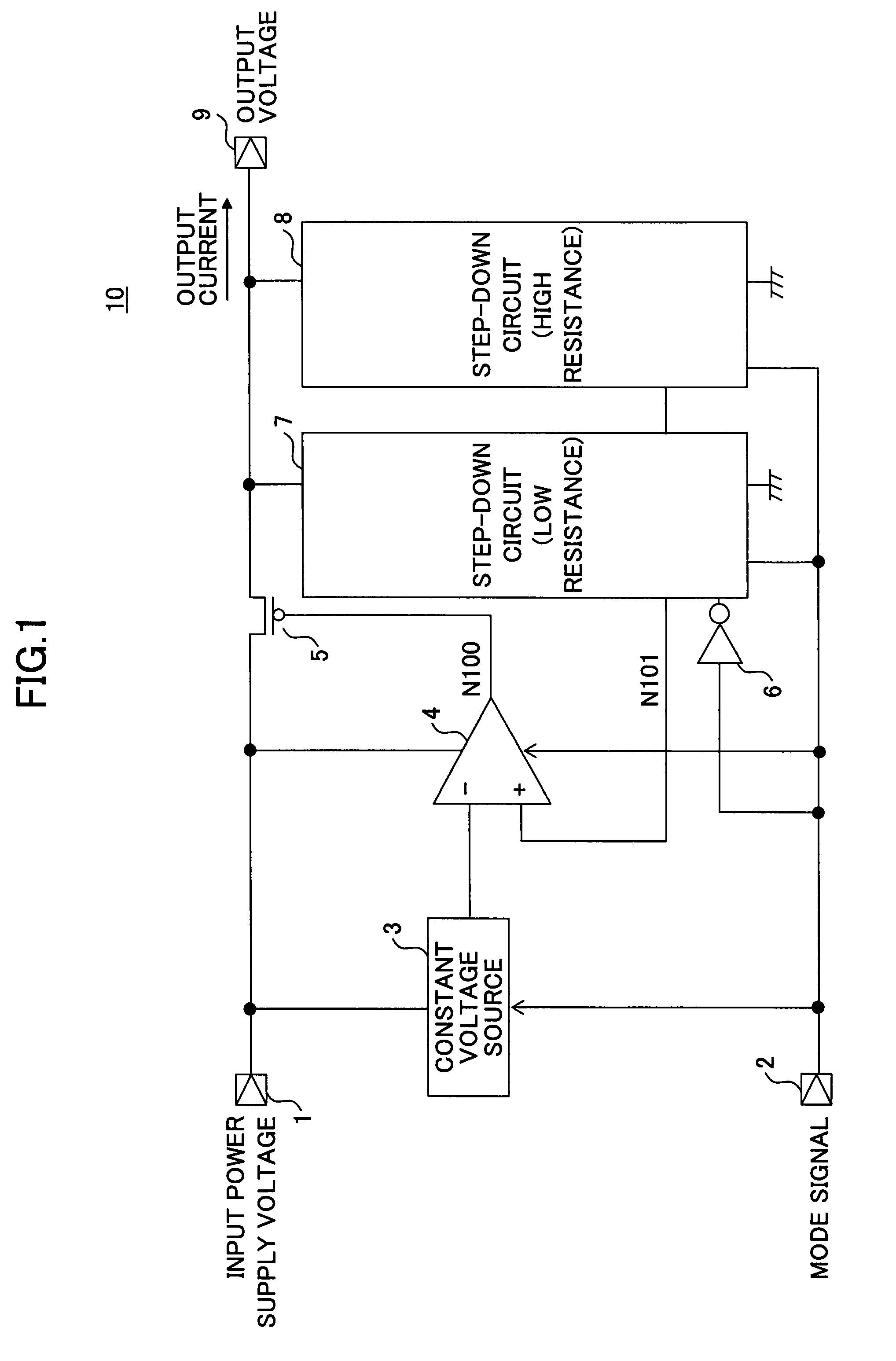
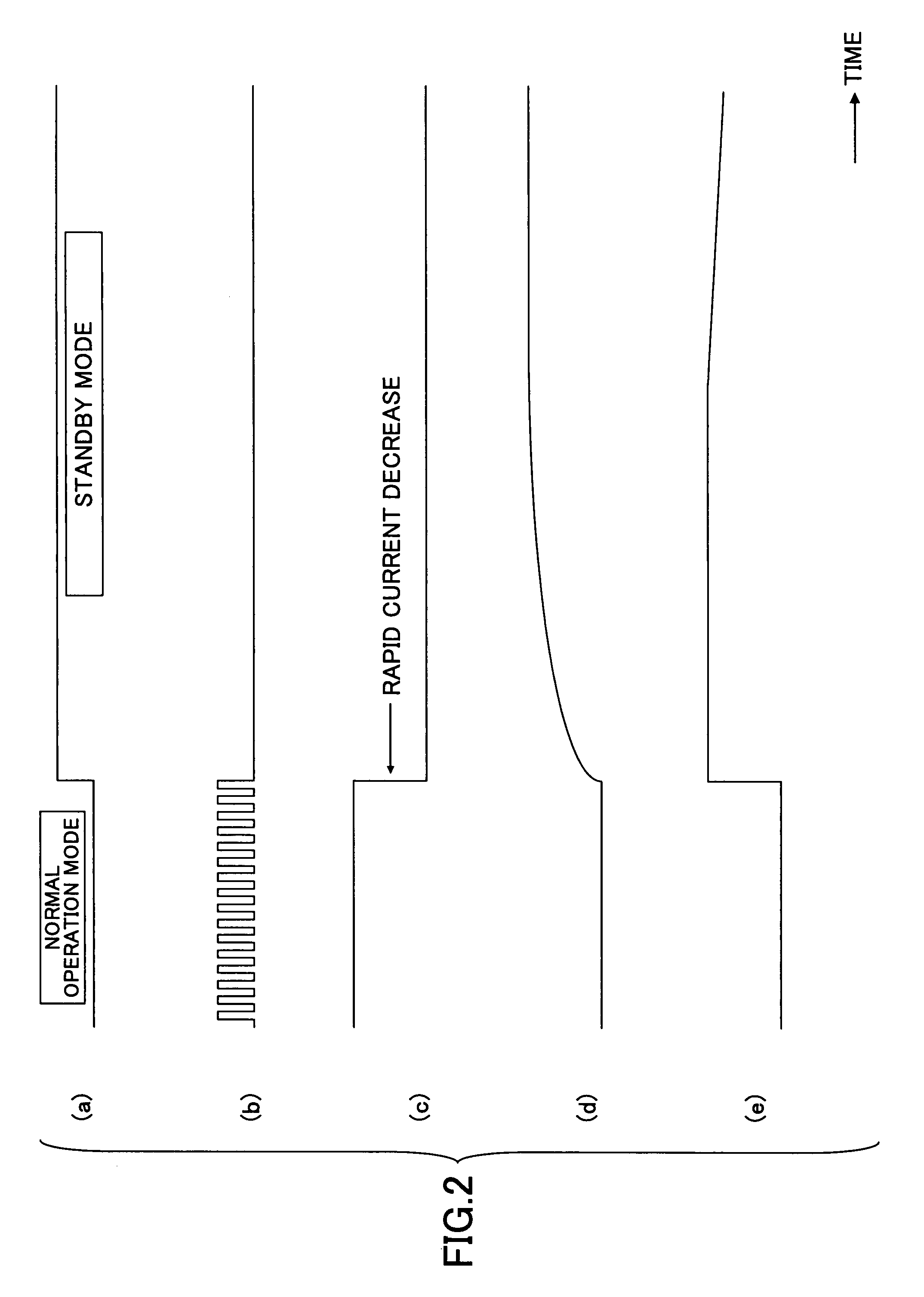
[0033]In the present invention, an LSI circuit is provided with a single power supply step-down circuit that integrally has a step-down circuit for a normal operation mode (or a first step-down circuit for a first operation mode) and a step-down circuit for a standby mode (or a second step-down circuit for a second operation mode) of the LSI circuit, so as to reduce the area occupied by the power supply step-down circuit. The current consumption of the LSI circuit is smaller in the standby mode than in the normal operation mode. The step-down circuit for the normal operation mode has a low (or lower) resistance, a high (or higher) reaction speed and a large (or larger) current consumption compared to the step-down circuit for the standby mode. The step-down circuit for the normal operation mode is activated only when the operation mode of the LSI circuit is the normal operation mode, so as to step down an input power supply voltage and to output an output voltage. On the other hand,...


PUM


Abstract

A power supply step-down circuit is adapted to a semiconductor integrated circuit having a first operation mode and a second operation mode having a smaller current consumption than the first operation mode. The power supply step-down circuit includes a first step-down circuit activated only during the first operation mode to step down an input power supply voltage to an output voltage, a second step-down circuit provided integrally with the first step-down circuit and activated only during the second operation mode to step down the input power supply voltage to an output voltage, an output terminal to output the output voltage of one of the first and second step-down circuits that is activated, and an output circuit to maintain the output voltage that is output from the output terminal lower than the input power supply voltage for a first predetermined time when an operation mode makes a transition from the first operation mode to the second operation mode.

Description

BACKGROUND OF THE INVENTION[0001]1. Field of the Invention[0002]The present invention generally relates to power supply step-down circuits and semiconductor devices, and more particularly to a power supply step-down circuit for stepping down an input power supply voltage and to a semiconductor device having such a power supply step-down circuit.[0003]2. Description of the Related Art[0004]Due to improvements made in the semiconductor producing processes that form extremely small patterns, the size of semiconductor integrated circuits (LSI circuits) within the semiconductor device has become extremely small, and voltages that may be applied to the LSI circuits have become low. On the other hand, from the point of view of the user of the LSI circuit, there are demands to use the same power supply voltage as the conventional LSI circuit, because of the desire to use the same power supply unit or the like as the conventional LSI circuit. Accordingly, a power supply step-down circuit is ...

Claims


Application Information

Patent Timeline
Patent Type & Authority Patents(United States)
IPC IPC(8): G05F1/613G05F3/16
CPCG05F1/56
Inventor KATO, TATSUO
Owner FUJITSU SEMICON LTD
Why Eureka
Try Eureka