Multilayer printed circuit board and manufacturing method thereof

a printed circuit board and multi-layer technology, applied in the direction of printed circuit parts, printed circuit stress/warp reduction, non-metallic protective coating applications, etc., can solve the problems of warping and deformation of printed circuit boards, electronic components are not securely bonded to the product parts, and it is difficult to solder electronic components to the product parts

Active Publication Date: 2009-03-03
FUJITSU LTD
View PDF11 Cites 49 Cited by
  • Summary
  • Abstract
  • Description
  • Claims
  • Application Information

AI Technical Summary

Benefits of technology

[0023]The above and other objects, features, advantages and technical and industrial significance of this invention will be better understood by reading the following detailed description of presently preferred embodiments of the invention, when considered in connection with the accompanying drawings.

Problems solved by technology

However, in the conventional technologies, warping and deformation of a printed circuit board still occurs due to heat of curing (thermosetting) in the reflow process.
If the printed circuit board warps, it is difficult to solder the electronic components to the product portions, and the electronic components are not securely bonded to the product portions.
This results in reduction in yield, quality, and reliability in manufacturing the printed circuit board is reduced.

Method used


Image

  • Multilayer printed circuit board and manufacturing method thereof
  • Multilayer printed circuit board and manufacturing method thereof
  • Multilayer printed circuit board and manufacturing method thereof

Examples


first embodiment

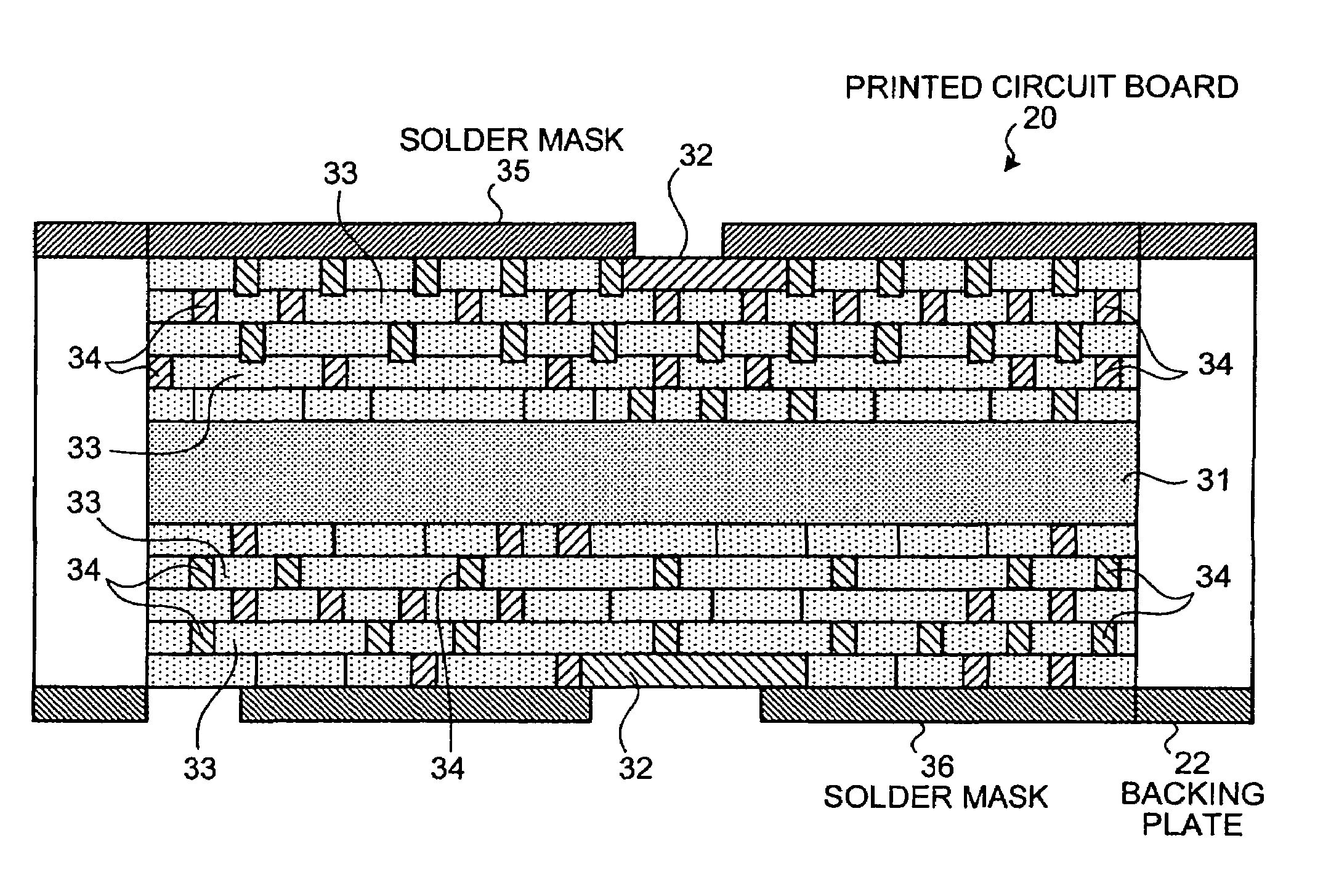
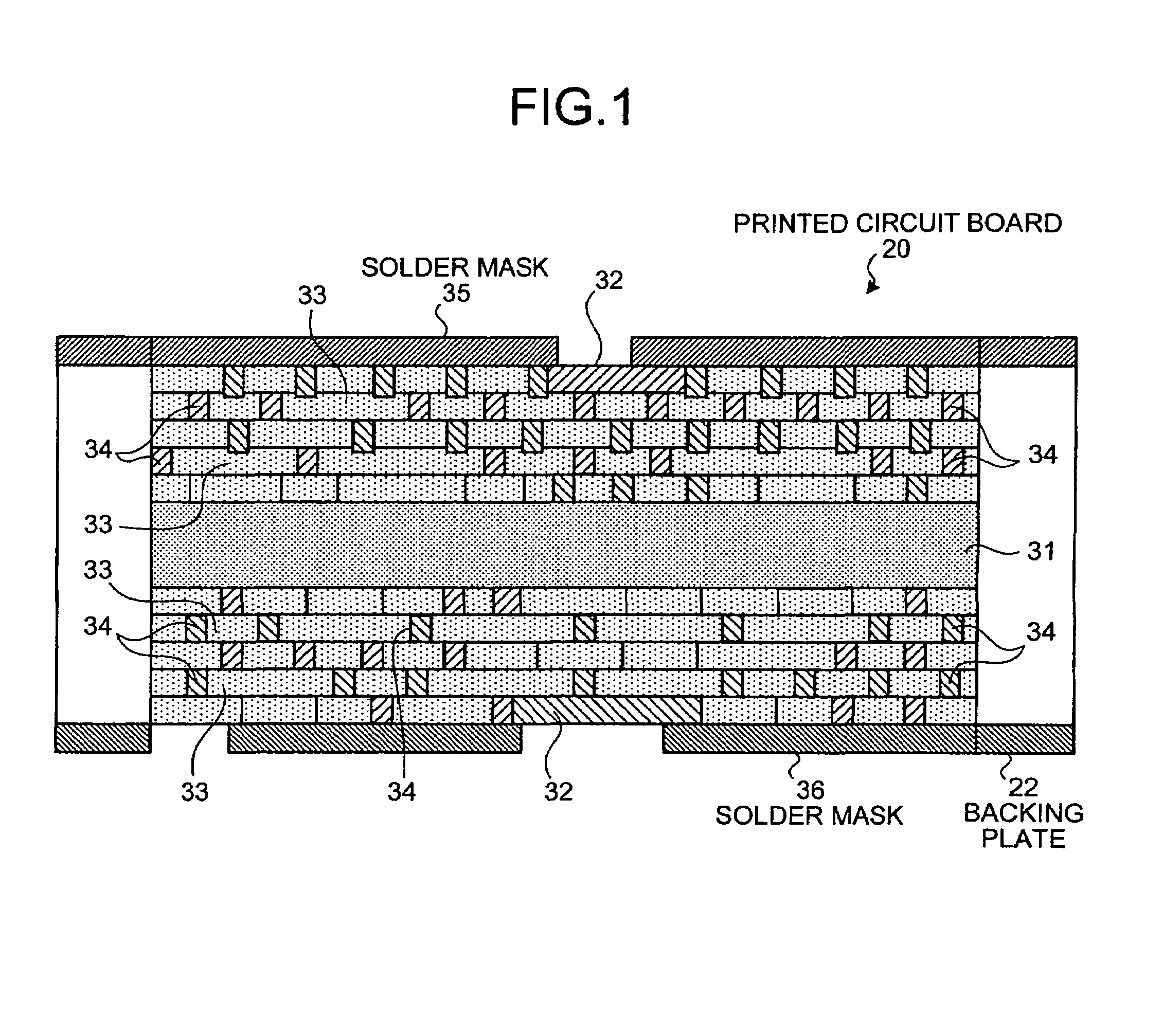
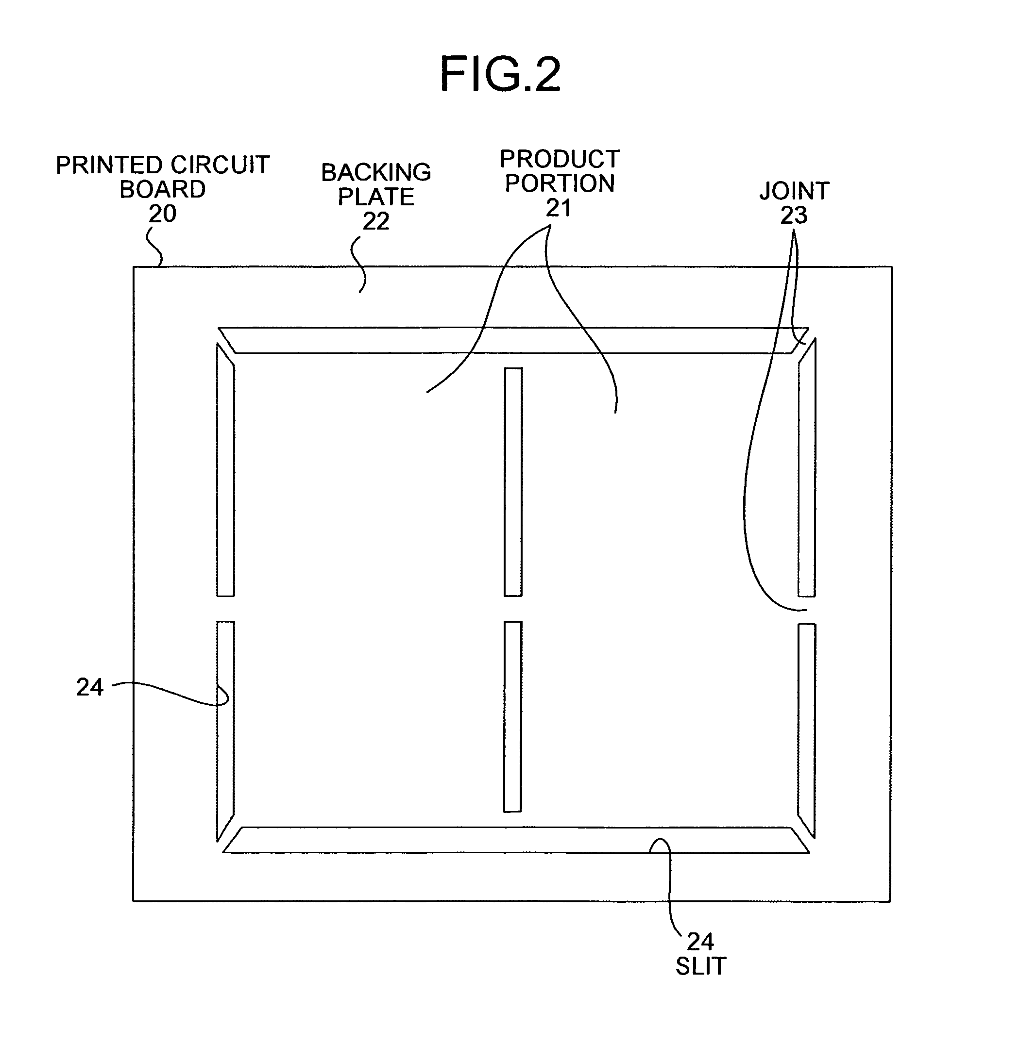
[0035]The outline of a structure of a multilayer printed circuit board 20 according to the present invention is explained with reference to FIGS. 1 and 2. FIG. 1 is a cross section of the multilayer printed circuit board 20, and FIG. 2 is a plan view of the multilayer printed circuit board 20.

[0036]The printed circuit board 20 includes product portions 21 with electronic components etc. mounted thereon, a backing plate 22 that is to be removed in manufacturing process, joints 23 formed on perforations, and slits 24. The product portions 21 are linked to the backing plate 22 by the joints 23. The upper and lower surfaces of the backing plate 22 are coated with solder mask 35 and solder mask 36 having different material characteristics, respectively. After the electronic components are soldered by the reflow process (heat fusing) onto a board, a predetermined number (two in the example of FIG. 2) of printed circuit boards can be obtained by a splitting process.

[0037]Further, as shown ...

second embodiment

[0048]A multilayer printed circuit board is explained next. FIG. 6 is a cross section of the multilayer printed circuit board, and FIG. 7 is a plan view of the multilayer printed circuit board.

[0049]In the printed circuit board 20 according to the first embodiment, the solder mask 35 and the solder mask 36 having different material characteristics are applied respectively to the upper and lower surfaces of the backing plate 22 that is linked to the product portions 21 by the joints 23. Thus, warping of the product portions 21 is suppressed. According to the second embodiment, however, based on the layout or wiring density of conductive circuit patterns, dummy vias (reinforcing members) are arranged in portions having less dense conductive circuit patterns. As a result, a uniform wiring density of the conductive circuit patterns is achieved, which enhances rigidity and suppresses warping.

[0050]In other words, a printed circuit board includes, due to circuitry, a portion where conduc...


PUM


Abstract

A printed circuit board includes a product portion and a backing plate. Upper and lower surfaces of the backing plate are coated with solder masks with different material characteristics.

Description

BACKGROUND OF THE INVENTION[0001]1. Field of the Invention[0002]The present invention relates to a multilayer printed circuit board, and a manufacturing method thereof.[0003]2. Description of the Related Art[0004]It has been common that, a printed circuit board has a multilayer (blind via hole (BVH)) structure including build-up layers to be mounted with electronic components such as semiconductor components etc. The multilayer printed circuit board includes multiple product portions linked with a portion that is to be removed in manufacturing process by joints. A plurality of semiconductor components can be intensively mounted on the product portions, which enhances mounting efficiency of the electronic components.[0005]An outline structure of a conventional multilayer printed circuit board 10 is explained with reference to FIGS. 8 and 9. FIG. 8 is a plan view of the multilayer printed circuit board 10, and FIG. 9 is a cross section of the multilayer printed circuit board 10.[0006]...

Claims


Application Information

Patent Timeline
Patent Type & Authority Patents(United States)
IPC IPC(8): H05K1/03
CPCH05K1/0271H05K3/0052H05K1/115H05K3/28H05K3/4602H05K2201/068H05K2201/09063H05K2201/0909H05K2201/09618H05K2201/09781H05K2201/2009H05K2203/1572H05K3/46
Inventor ITOH, NOBUTAKA
Owner FUJITSU LTD
Why Eureka
Try Eureka