Supercharge Your Innovation With Domain-Expert AI Agents!

Phase change memory devices and program methods

a memory device and phase change technology, applied in the direction of information storage, static storage, digital storage, etc., can solve the problem of unnecessari consumption of current through the second current path of about 0.12 milliamper

Active Publication Date: 2009-03-03
SAMSUNG ELECTRONICS CO LTD
View PDF22 Cites 9 Cited by
  • Summary
  • Abstract
  • Description
  • Claims
  • Application Information

AI Technical Summary

Benefits of technology

The invention is a phase change memory device that includes a memory cell array and a write driver circuit. The write driver circuit provides a set current and a reset current to a selected memory cell. The method of programming the device involves receiving a set pulse or a reset pulse based on the input data, generating a reset control signal, and receiving a reset DC voltage to provide the reset current to the selected memory cell. The technical effect of this invention is to improve the programming accuracy and reliability of phase change memory devices.

Problems solved by technology

In the above-described example, although the conventional write driver requires a current of about 1 milliampere in the reset program operation, there is a problem in that a current of about 0.12 milliampere is unnecessarily consumed through the second current path.

Method used


Image

  • Phase change memory devices and program methods
  • Phase change memory devices and program methods
  • Phase change memory devices and program methods

Examples


Embodiment Construction

[0030]Embodiments of the invention will now be described in some additional detail with reference to the accompanying drawings. Throughout the written description and drawings, like reference numbers indicate like or similar elements.

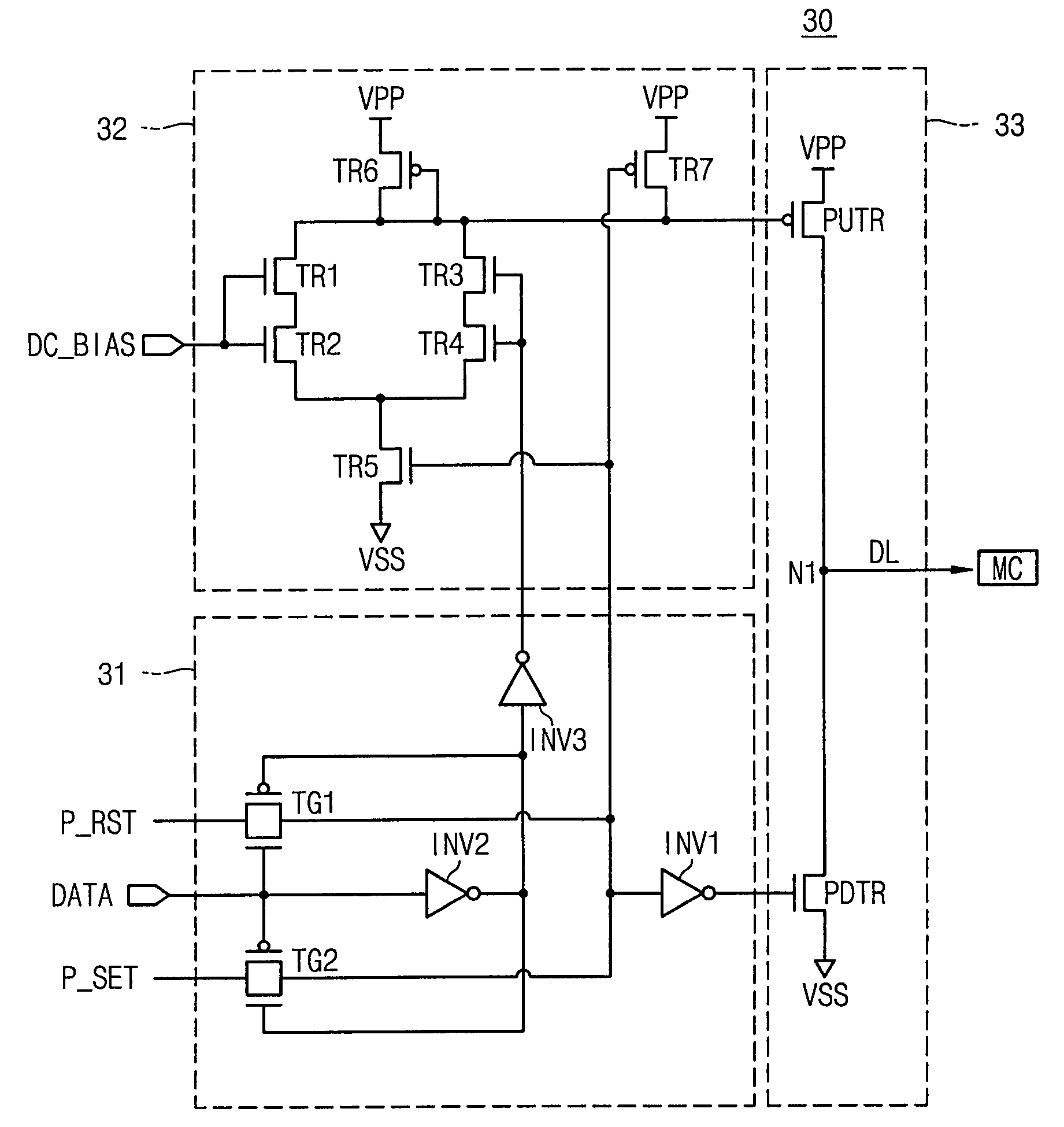
[0031]FIG. 5 is a block diagram illustrating a phase change memory device 100 according to an embodiment of the invention. Referring to FIG. 5, phase change memory device 100 includes a memory cell array 110, an address decoder 102, a bitline selection circuit 130, a write driver circuit 140 and a control unit 150.

[0032]Memory cell array 110 includes a plurality of memory cells. Each of the memory cells is configured with a memory element and a select element. The memory element includes a phase change material, such as a GST, and the select element, such as a diode D (as represented in FIG. 5) or alternately an NMOS transistor.

[0033]Address decoder 120 is connected to memory cell array 110 via wordlines WL0˜WLn. Address decoder 120 decodes an externall...


PUM


Abstract

A phase change memory device is disclosed. It includes a memory cell array including a plurality of memory cells programmed in relation to a phase change material, and a write driver circuit configured to provide a set current and a reset current to a selected memory cell. The write driver circuit includes a set current driver configured to provide the set current and a reset current driver configured to provide the reset current.

Description

STATEMENT OF RELATED APPLICATIONS[0001]This application is a Continuation in Part (CIP) of U.S. patent application Ser. No. 11 / 724,268, filed Mar. 15, 2007. A claim of priority under 35 U.S.C. § 119 is made to Korean Patent Application No. 2006-029692 filed on Mar. 31, 2006 and Korean Patent Application No. 2006-132684 filed Dec. 22, 2006, the collective subject matter of which is hereby incorporated by reference.BACKGROUND OF THE INVENTION[0002]1. Field of the Invention[0003]The present invention relates to nonvolatile semiconductor memory devices. More particularly, the invention relates to phase change memory devices and methods for applying a program current.[0004]2. Discussion of Related Art[0005]Phase change memory devices are one class of nonvolatile memory devices. Instead of storing electrical charge to indicate a date value, as is done in other nonvolatile memory devices, the state of a phase change material, such as Ge—Sb—Te (GST), is used to indicate a data value.[0006]F...

Claims


Application Information

Patent Timeline
Patent Type & Authority Patents(United States)
IPC IPC(8): G11C11/00
CPCG11C13/0004G11C13/0069G11C2013/0078G11C2213/72
Inventor CHOI, BYUNG-GILKIM, DU-EUNGRO, YU-HWANCHOI, JOON-YONGCHO, BEAK-HYUNGCHO, WOO-YEONG
Owner SAMSUNG ELECTRONICS CO LTD
Features
  • R&D
  • Intellectual Property
  • Life Sciences
  • Materials
  • Tech Scout
  • Unparalleled Data Quality
  • Higher Quality Content
  • 60% Fewer Hallucinations
Learn More