Charge pump circuit

a pump circuit and discharge pump technology, applied in the direction of power conversion systems, instruments, dc-dc conversion, etc., can solve the problems of incorrect pixel data, affecting the affecting the grey scale performance and image quality of the display panel, so as to reduce the noise caused by voltage spikes

Inactive Publication Date: 2009-03-31
NOVATEK MICROELECTRONICS CORP
View PDF2 Cites 15 Cited by
  • Summary
  • Abstract
  • Description
  • Claims
  • Application Information

AI Technical Summary

Benefits of technology

[0012]Accordingly, the present invention is directed to a charge pump circuit, wherein the turn-on speeds of switches are controlled so that the equivalent impedances of the switches change from high values to low values when the switches transmit from off state to on state, and accordingly the voltage change of a capacitor can be slowed down and noises caused by voltage spikes can be reduced during a charging procedure and the output of the charge pump circuit can be stabilized.
[0014]The present invention provides a charge pump circuit including a plurality of switches and a switch control circuit. The charge pump circuit is suitable for a display panel. The switch control circuit is coupled to the switches for controlling the on / off states of the switches and allowing the charge pump circuit to provide an output voltage different from an input voltage. The switch control circuit prolongs the time required for enable transition of the switches than the time required for disable transition thereof, wherein the equivalent impedances of the switches change from high values to low values when the switches are at enable transition.
[0016]The present invention further provides a charge pump circuit including a plurality of switches, a switch driving circuit, and a clock generating circuit. The charge pump circuit is suitable for a display panel. The switch driving circuit is coupled to the switches for receiving a first clock signal and outputs a second clock signal for controlling the on / off states of the switches. The clock generating circuit is coupled to the switch driving circuit for generating the first clock signal and allowing the charge pump circuit to provide an output voltage different from an input voltage. The switch driving circuit prolongs the time required for enable transition of the switches longer than the time required for disable transition thereof. The equivalent impedances of the switches change from high values to low values when the switches are at enable transition.
[0019]In the present invention, a switch control circuit is adopted in a charge pump circuit for controlling the on / off states of a plurality of switches and allowing the charge pump circuit to provide an output voltage that is different from an input voltage. The switch control circuit makes the time required for enable transition of the switches longer than the time required for disable transition thereof. When the switches are at enable transition, the equivalent impedances of the switches change from high values to low values, so that the transient change in the voltage over the capacitor during charge / discharge procedure is slowed down and accordingly noises caused by voltage spikes are reduced and output voltage is stabilized.

Problems solved by technology

When a conventional charge pump circuit is applied to a small-size display panel, voltage spikes are produced at instances when switches are enabled, so that the common voltage in the display panel is disturbed and accordingly the pixel quality of the display panel is affected.
However, such increase in working frequencies of the clock signals may cause increase in voltage spikes and coupling between voltage spikes and some of the pixel data, therefore incorrect pixel data will be produced and both grey scale performance and image quality of the display panel will be affected.
However, when applied to a display panel, the working frequency of the charge pump circuit has to be increased due to insufficient driving capability of the minimized charge pump circuit, and such increase in working frequency may produce more continuous voltage spikes and accordingly affect the display quality of the display panel.

Method used


Image

  • Charge pump circuit
  • Charge pump circuit
  • Charge pump circuit

Examples


Embodiment Construction

[0028]Reference will now be made in detail to the present embodiments of the invention, examples of which are illustrated in the accompanying drawings. Wherever possible, the same reference numbers are used in the drawings and the description to refer to the same or like parts.

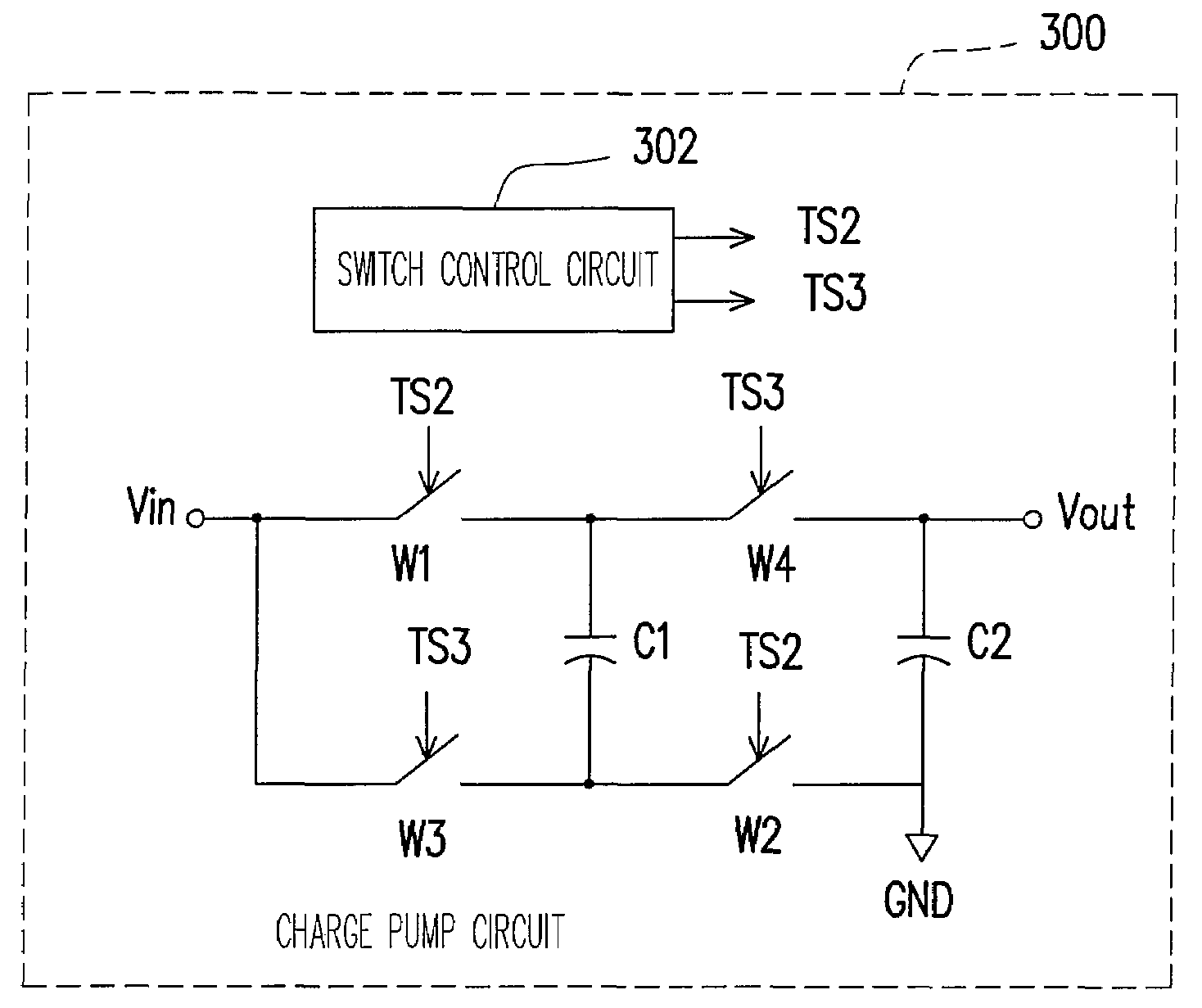
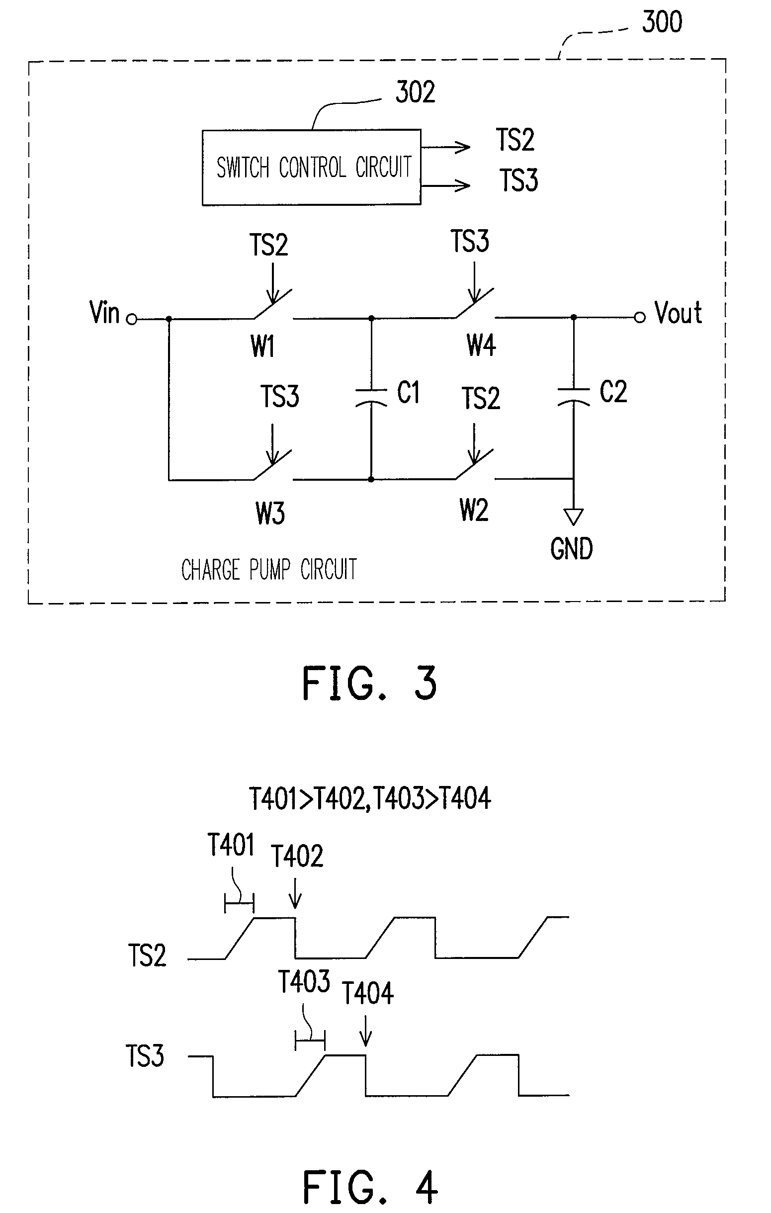
[0029]FIG. 3 illustrates a charge pump circuit according to an embodiment of the present invention. Referring to FIG. 3, the charge pump circuit 300 is suitable for a display panel, which includes a switch control circuit 302, switches W1˜W4, a capacitor C1, and a capacitor C2, wherein each of the switches W1˜W4 has a first terminal, a second terminal, and a control terminal, and each capacitor has a first terminal and a second terminal. The couplings between foregoing components will be described herein. The first terminal of the switch W1 is coupled to an input voltage Vin, and the second terminal of the switch W1 is coupled to the first terminal of the switch W4 and the first terminal of the capacitor C1. T...


PUM


Abstract

A charge pump circuit including a plurality of switches and a switch control circuit is provided. The charge pump circuit is suitable for a display panel. The switches switch from “off” state to “on” state in an enable transition, and switch from “on” state to “off” state in a disable transition. The switch control circuit is coupled to the switches for controlling the on / off states of the switches and allowing the charge pump circuit to provide an output voltage that is different from an input voltage. The switch control circuit prolongs the time required for enable transition of the switches to be longer than the time for disable transition thereof. The equivalent impedances of the switches change from high values to low values when the switches are at the enable transition.

Description

CROSS-REFERENCE TO RELATED APPLICATION[0001]This application claims the priority benefit of Taiwan application serial no. 96109468, filed Mar. 20, 2007. All disclosure of the Taiwan application is incorporated herein by reference.BACKGROUND OF THE INVENTION[0002]1. Field of the Invention[0003]The present invention generally relates to a charge pump circuit, and more particularly, to a charge pump circuit which can reduce voltage spike.[0004]2. Description of Related Art[0005]Various voltage source levels are usually required in an electronic apparatus, thus, a charge pump circuit is usually employed to generate voltage sources of different levels. Plural charge pump circuits are applied in power supply circuit of display panel.[0006]FIG. 1 illustrates a conventional charge pump circuit. Referring to FIG. 1, the charge pump circuit 100 includes a switch control circuit 102, switches 104˜107, a capacitor CS, and a capacitor CL. The conventional switch control circuit 102 generates two...

Claims


Application Information

Patent Timeline
Patent Type & Authority Patents(United States)
IPC IPC(8): G05F1/10G05F3/02
CPCH02M3/07
Inventor YEN, CHIH-JENHSIEH, CHIH-YUAN
Owner NOVATEK MICROELECTRONICS CORP
Why Eureka
Try Eureka