Semiconductor device and power supply device using the same

a technology of semiconductor devices and power supply devices, applied in the direction of dc-dc conversion, solid-state devices, power electronics conversion efficiency, etc., can solve the problems of large inductance, reduce the inductance of the main circuit of the semiconductor device, reduce the loss of power sources, and reduce voltage spikes

Active Publication Date: 2009-01-20
RENESAS ELECTRONICS CORP
View PDF2 Cites 7 Cited by
  • Summary
  • Abstract
  • Description
  • Claims
  • Application Information

AI Technical Summary

Benefits of technology

[0013]Accordingly, the present invention has been made to solve the above problem, and an object of the present invention is to provide a semiconductor device capable of reducing an inductance.
[0018]The present invention has the effect that the inductance of the main circuit of the semiconductor device is reduced and thereby a power source loss and a voltage spike can be reduced.

Problems solved by technology

Therefore, there is a problem of the inductance being large.

Method used


Image

  • Semiconductor device and power supply device using the same
  • Semiconductor device and power supply device using the same
  • Semiconductor device and power supply device using the same

Examples


first embodiment

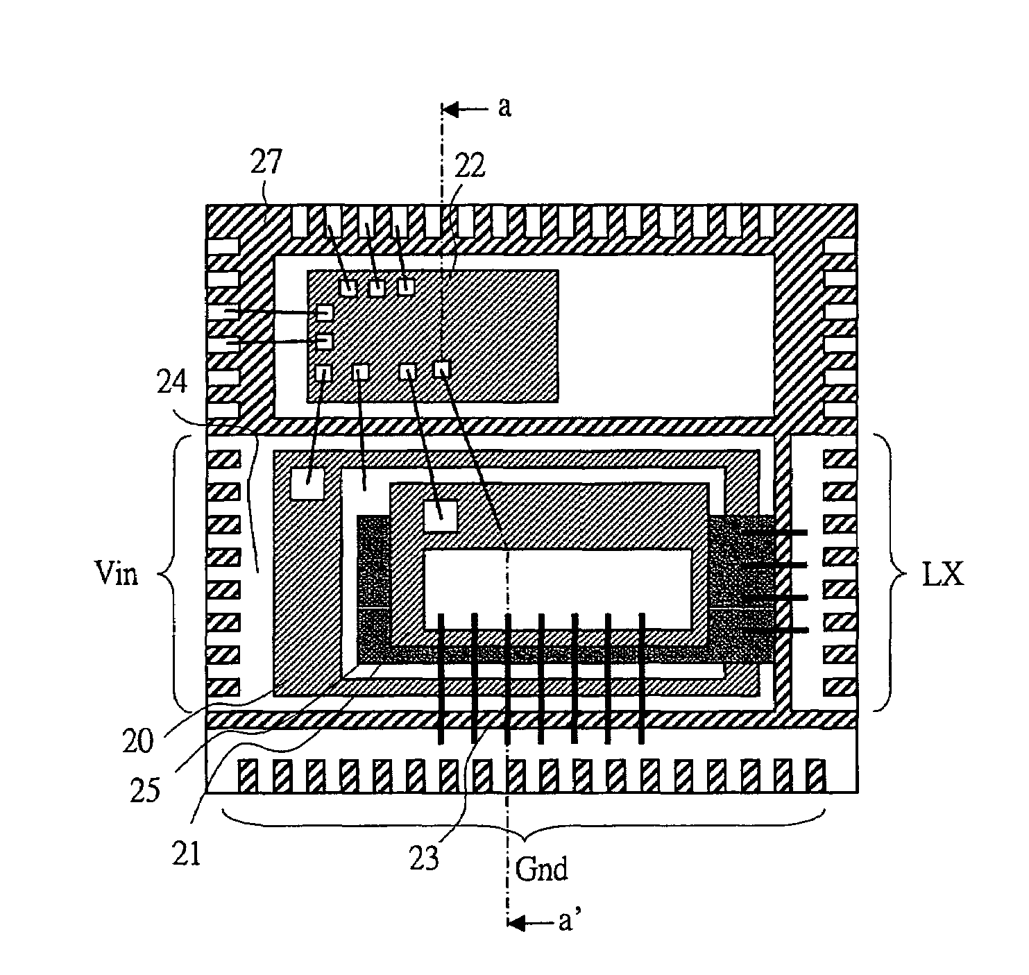
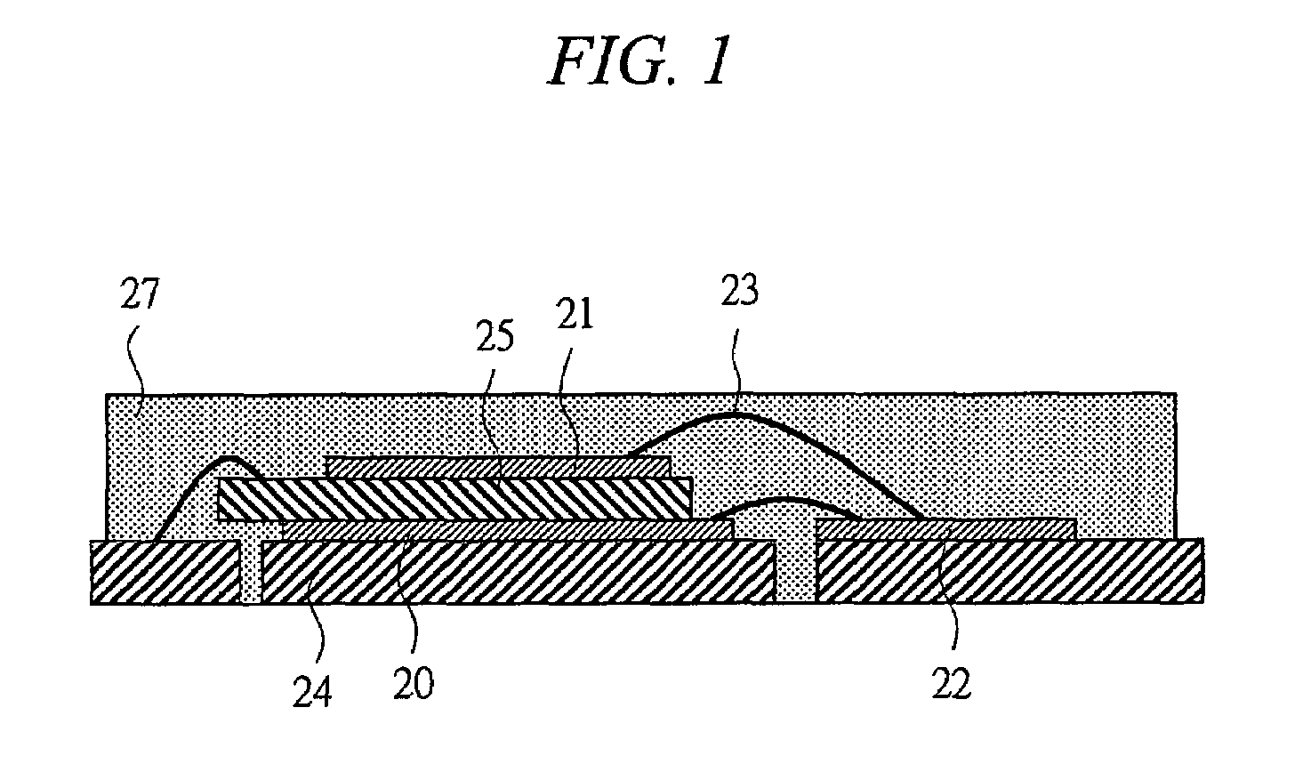
[0053]By using FIG. 12 and FIG. 1, a semiconductor device according to a first embodiment of the present invention is described. As shown in FIG. 12, the semiconductor device according to the present embodiment includes the rectification MOSFET 20, the commutation MOSFET 21, and the driving Integrated Circuit (IC) 22 that drives these MOSFETs. The rectification MOSFET 20, a metal plate (conductive member) 25, and the commutation MOSFET 21 are laminated. Through the wire bondings 23, the driving IC 22, the rectification MOSFET 20, and the commutation MOSFET 21 are connected. The rectification MOSFET 20 and a lead frame that leads to output terminals LX are connected to the metal plate through the wire bondings. The commutation MOSFET 21 and a lead frame that leads to ground terminals Gnd are connected through the wire bondings. The terminals of the main circuit and the terminals of the driving IC are placed on the same plane. This is because since the semiconductor device according t...

second embodiment

[0056]Next, an embodiment in which a stress of the metal plate 25 is mitigated is described. In a step of manufacturing the semiconductor device according to the present invention, a high-temperature process called a reflow is involved. At a time of performing the reflow, since a coefficient of thermal expansion of the semiconductor is different from that of the metal, there are problems of, for example, an occurrence of crack in a semiconductor chip. In the embodiment of FIG. 14, a plurality of trenches 46 are provided in the metal plate 25, thereby making it possible to mitigate the stress caused at the time of performing the reflow.

third embodiment

[0057]Next, another embodiment in which the inductance can be further reduced as compared with the first embodiment is described. In FIG. 12, the wire bondings are used for connections from the metal plate 25 to the lead frame 24 and from the commutation MOSFET 21 to the ground terminals. However, there is a problem in which the inductance of the wire bonding is larger than that of the metal plate.

[0058]FIG. 15 depicts an embodiment in which the metal plate 25 and a metal plate 28 are used for connections from the metal plate 25 to the lead frame 24 and from the commutation MOSFET 21 to the ground terminals, whereby as compared with the first embodiment, the inductance of the main circuit can be significantly reduced. FIG. 16 is a section view of FIG. 15 (taken along line a-a′).

[0059]In the present embodiment, the metal plates are used for connections from the metal plate 25 to the lead frame 24 and from the commutation MOSFET 21 to the ground terminals. Alternatively, the metal pla...


PUM


Abstract

A semiconductor device capable of reducing an inductance is provided. In the semiconductor device in which a rectification MOSFET, a commutation MOSFET, and a driving IC that drives these MOSFETs are mounted on one package, the rectification MOSFET, a metal plate, and the commutation MOSFET are laminated. A current of a main circuit flows from a back surface of the package to a front surface thereof. The metal plate is connected to an output terminal via a wiring in the package. Wire bondings are used for wirings for connecting the driving IC, the rectification MOSFET, and the commutation MOSFET, all terminals being placed on the same plane. For this reason, the inductance becomes small and also a power source loss and a spike voltage are reduced.

Description

CROSS-REFERENCE TO RELATED APPLICATION[0001]The present application claims priority from Japanese patent application No. JP 2005-307999 filed on Oct. 24, 2005, the content of which is hereby incorporated by reference into this application.BACKGROUND OF THE INVENTION[0002]The present invention relates to a power supply device and, particularly, to a technology effectively applicable to a semiconductor device and a power supply device for use in electronic equipment or the like.[0003]Conventionally, as a power supply device for use in electronic equipment or the like, a power supply device as shown in FIG. 2 is known. In the power supply device shown in FIG. 2, a direct-current power inputted to an input unit 51, which is configured to include an input capacitor 61, from a direct-current input power source 60 is switched by a switching unit 52 based on a control signal outputted from a driving unit 70. Power is supplied to a load 66 from an output unit 53 configured to include a commu...

Claims


Application Information

Patent Timeline
Patent Type & Authority Patents(United States)
IPC IPC(8): H02M1/00
CPCH01L25/074H01L25/16H01L2224/48091H01L2224/48137H01L2924/3011H02M3/1588H01L2224/4903H01L2224/49175H01L2924/13091H01L2924/30107H01L2924/12032H01L2224/05554H01L2224/0603H01L2924/181H01L2224/40245H01L2924/00014Y02B70/10H01L2924/00H01L2924/00012H01L2224/37099
Inventor HASHIMOTO, TAKAYUKIMATSUURA, NOBUYOSHISHIRAISHI, MASAKISATOU, YUKIHIROKAWASHIMA, TETSUYA
Owner RENESAS ELECTRONICS CORP
Why Eureka
Try Eureka