Liquid crystal electro-optical device and method of driving the same

a technology of electrooptical devices and liquid crystals, applied in liquid crystal compositions, instruments, chemistry apparatuses and processes, etc., can solve problems such as unintended color display, display dark, display in unintended colors, etc., and achieve the effect of efficient utilization of light and superior viewing angl

Inactive Publication Date: 2009-03-31
SEMICON ENERGY LAB CO LTD
View PDF58 Cites 34 Cited by
  • Summary
  • Abstract
  • Description
  • Claims
  • Application Information

AI Technical Summary

Benefits of technology

[0023]An object of the present invention is to provide, by solving the above problems, a liquid crystal electro-optical device which has both of the advantage of the IPS mode, i.e., the superior viewing angle characteristic and the advantage of the guest-host mode, i.e., the efficient utilization of light.

Problems solved by technology

However, in the liquid crystal electro-optical device which operates in the above manner, although a normal display state can be obtained when it is viewed from the direction perpendicular to the display screen, it exhibits dark, unclear display when viewed obliquely.
In the case of color display, oblique viewing causes display in an unintended color.
Thus, the viewing angle characteristic with respect to a viewer such that the performance deteriorates as the viewing direction deviates from the perpendicular direction.
This is caused by voltage non-application / application switching.
As a result, the above-mentioned viewing angle problem occurs even in the guest-host type liquid crystal electro-optical devices.
As described above, although the liquid crystal electro-optical device that operates in the IPS mode has the advantage of a wide viewing angle, it is disadvantageous in that the brightness is low due to the use of a polarizing plate.
However, like other conventional liquid crystal electro-optical devices, this mode has the problem of a strong dependence on the viewing angle.

Method used


Image

  • Liquid crystal electro-optical device and method of driving the same
  • Liquid crystal electro-optical device and method of driving the same
  • Liquid crystal electro-optical device and method of driving the same

Examples


Embodiment Construction

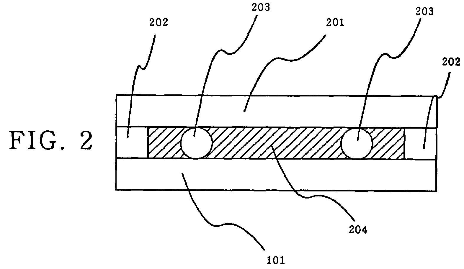
[0032]FIG. 2 show a specific configuration of a liquid crystal electro-optical device according to an example of the present invention.

[0033]In FIG. 2, each of a first substrate 101 and a second substrate 201 is transparent and is made of a material having a certain level of strength with respect to external force, examples of which are inorganic materials such as glass and quartz.

[0034]A liquid crystal material serving as a light modulating layer 204 is interposed between the substrates 101 and 201. The liquid crystal material is a liquid crystal containing a dichroic dye and an optically active substance therein.

[0035]A metal material such as copper, aluminum, tantalum, titanium, or chromium, and a silicide material are used as an electric field applying means. Other examples of the electric field applying means are transparent conductive materials such as ITO (indium tin oxide), tin oxide, and indium oxide.

[0036]A sealing member 202 is formed into a desired pattern to serve as an...


PUM

PropertyMeasurementUnit
thicknessaaaaaaaaaa
interelectrode distanceaaaaaaaaaa
thicknessaaaaaaaaaa

Abstract

An electric field that is parallel with a TFT substrate is formed by a pair of electrodes formed on the TFT substrate. Liquid crystal molecules in a light modulating layer are caused to respond electro-optically to the electric field. The light modulating layer is constituted of a liquid crystal material, an optically active substance, and a dichroic dye. The spiral pitch p [μm] of the light modulating layer, the cell thickness d [μm], the twist angle n of liquid crystal molecules, and the interelectrode interval L [μm] are set in ranges of 1≦p≦15, 1≦d≦10, n≦300°, and L<25.

Description

CROSS-REFERENCE TO RELATED APPLICATIONS[0001]This application is a divisional application of U.S. application Ser. No. 09 / 280,185, filed on Mar. 29, 1999, now U.S. Pat. No. 6,697,129, which is a continuation of U.S. application Ser. No. 08 / 799,985, filed on Feb. 12, 1997, now U.S. Pat. No. 6,055,028, which claims the benefit of a foreign priority application filed in Japan, on Feb. 14, 1996, as serial number 08-52405. This application claims priority to all of these applications, and all of these applications are incorporated by reference.BACKGROUND OF THE INVENTION[0002]1. Field of the Invention[0003]The present invention relates to a liquid crystal electro-optical device which is superior in both electrical characteristics and contrast and which can provide bright and uniform display over the entire screen.[0004]2. Description of the Related Art[0005]A liquid crystal electro-optical device is constructed such that a liquid crystal material, which is generally an organic material, ...

Claims


Application Information

Patent Timeline
Patent Type & Authority Patents(United States)
IPC IPC(8): G02F1/133C09K19/02G02F1/1335G02F1/1343G02F1/139
CPCG02F1/134363G02F1/13725G02F1/1397
Inventor NISHI, TAKESHISATAKE, RUMOHIRAKATA, YOSHIHARU
Owner SEMICON ENERGY LAB CO LTD
Why Eureka
Try Eureka