Method of forming a cavity by two-step etching and method of reducing dimension of a MEMS device

a two-step etching and cavity technology, applied in the manufacture of microstructural devices, microstructures, microstructures, etc., can solve the problems of waste of available areas on single crystalline silicon substrates, redundancy size c is not functional for piezoresistive pressure sensors, etc., to reduce the dimension of a mems device and improve integration

Inactive Publication Date: 2009-04-07
TOUCH MICRO SYST TECH
View PDF2 Cites 20 Cited by
  • Summary
  • Abstract
  • Description
  • Claims
  • Application Information

AI Technical Summary

Benefits of technology

[0006]It is therefore one of the objectives of the claimed invention to provide a method of form a cavity by two-step etching and reducing the dimension of a MEMS device to improve the integration.
[0008]According to the claimed invention, a method of reducing a dimension of a MEMS device is provided. First, a single crystalline silicon substrate having a diaphragm disposed on a front surface is provided. Then, a first-step anisotropic dry etching process is performed to etch a back surface of the single crystalline silicon substrate to form an opening corresponding to the diaphragm. The etching of the single crystalline silicon substrate stops on a specific lattice plane extending from edges of the diaphragm. Subsequently, a second-step anisotropic wet etching process is performed to etch the single crystalline silicon substrate along the specific lattice plane until the diaphragm is exposed to form a cavity. The cavity has a diamond-like shape.

Problems solved by technology

This redundant size C is not functional for the piezoresistive pressure sensor 10, but wastes the available areas on the single crystalline silicon substrate 12.

Method used


Image

  • Method of forming a cavity by two-step etching and method of reducing dimension of a MEMS device
  • Method of forming a cavity by two-step etching and method of reducing dimension of a MEMS device
  • Method of forming a cavity by two-step etching and method of reducing dimension of a MEMS device

Examples


Embodiment Construction

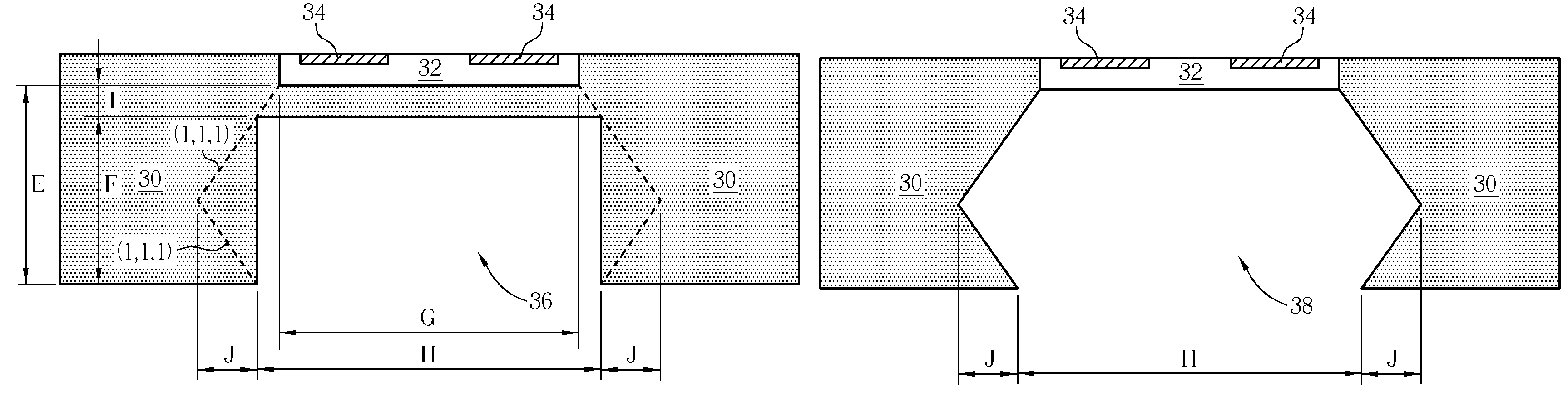
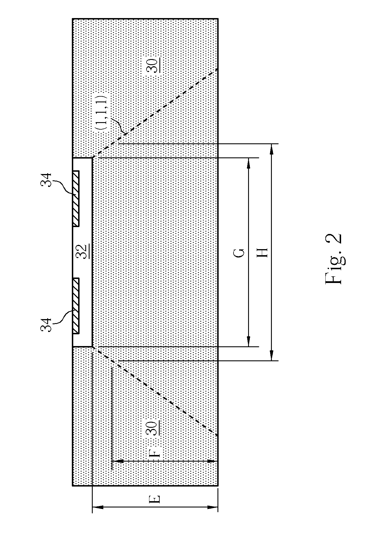
[0012]Refer to FIG. 2 to FIG. 5. FIG. 2 to FIG. 5 are schematic diagrams illustrating a method of reducing a dimension of a MEMS device according to a preferred embodiment of the present invention. According to the method of the present invention, the cavity of the MEMS device is accomplished by two-step etching, and only a single piezoresistive pressure sensor is illustrated for highlighting the feature of the present invention. As shown in FIG. 2, a single crystalline silicon substrate 30 e.g. a single crystalline silicon wafer is provided. The single crystalline silicon substrate 30 has a specific lattice orientation such as (1,0,0). The single crystalline silicon substrate 30 includes a diaphragm 32 disposed on the front surface, and a plurality of piezoresistors 34 formed in the diaphragm 32 to convert pressure signals into voltage signals. For a piezoresistive pressure sensor, the piezoresistors 34 are connected as a Wheaston bridge so as to amplify voltage signals.

[0013]The d...


PUM


Abstract

A method for reducing dimension of an MEMS device. A single crystalline substrate having a diaphragm is provided. A first-step anisotropic dry etching process is performed to form an opening corresponding to the diaphragm in the back surface, the anisotropic dry etching stopping on a specific lattice plane extending from the edge of the diaphragm. A second-step anisotropic wet etching process is performed to etch the single crystalline substrate along the specific lattice plane until the diaphragm is exposed to form a cavity having a diamond-like shape.

Description

BACKGROUND OF THE INVENTION[0001]1. Field of the Invention[0002]The present invention relates to a method of forming a cavity by two-step etching, and more particularly, to a method of forming a cavity having a diamond-like shape by two-step etching that can effectively reduce the dimension of a MEMS device.[0003]2. Description of the Prior Art[0004]Refer to FIG. 1. FIG. 1 is a schematic diagram of a conventional piezoresistive pressure sensor. As shown in FIG. 1, the conventional piezoresistive pressure sensor 10 includes a single crystalline silicon substrate 12, a diaphragm 14 disposed on the front surface of the single crystalline silicon substrate 12, a plurality of piezoresistors 16 formed in the diaphragm 14, and a cavity (back chamber) 18 formed on the back surface of the single crystalline silicon substrate 12. The cavity 18 enables the diaphragm 14 to be suspended, so that the diaphragm 14 can provide a pressure-sensing function. It is appreciated that the cavity 18 of the...

Claims


Application Information

Patent Timeline
Patent Type & Authority Patents(United States)
IPC IPC(8): H01L21/00
CPCB81C1/00587B81C2201/0133
Inventor HUANG, TER-CHANGLIN, HUNG-YIHSU, WEN-SYANG
Owner TOUCH MICRO SYST TECH
Why Eureka
Try Eureka