Liquid crystal display device with high aperture ratio having a metal layer and a storage electrode entirely overlapped with a common electrode

a liquid crystal display and high aperture ratio technology, applied in non-linear optics, instruments, optics, etc., can solve the problems of poor viewing angle characteristics and the central region of the electrodes not helping to increase the aperture ratio, so as to reduce the area ratio and enhance the aperture ratio

Active Publication Date: 2009-04-07
LG DISPLAY CO LTD
View PDF8 Cites 30 Cited by
  • Summary
  • Abstract
  • Description
  • Claims
  • Application Information

AI Technical Summary

Benefits of technology

[0019]An advantage of the present invention is to provide an LCD (Liquid Crystal Display) device capable of reducing an area ratio assumed by a light blocking region in a unit pixel region and enhancing an aperture ratio by forming a storage capacitor, namely, a light blocking region, to overlap with a lower end of at least one electrode.
[0020]To achieve these and other advantages and in accordance with the purpose of the present invention, as embodied and broadly described herein, there is provided an in-plane switching (IPS) mode liquid crystal display (LCD) device including: first and second substrates; a gate line and a data line arranged horizontally and vertically to define a plurality of pixel regions on the first substrate; a switching device, having a gate electrode, a semiconductor layer and source and drain electrodes, at a crossing of the gate line and the data line; a passivation film on an entire surface of the first substrate including the switching device; a common electrode and a pixel electrode arranged in an alternating pattern at an upper portion of the passivation film, wherein an in-plane electric field is generated between the common and pixel electrodes and at least one of the common and pixel electrodes has a first storage capacitor at its lower end; and a liquid crystal layer between the first and second substrates.
[0021]In another aspect of the present invention, there is provided an in-plane switching (IPS) mode liquid crystal display (LCD) device including: first and second substrates; a gate line and a data line arranged horizontally and vertically to define a plurality of pixel regions on the first substrate; a switching device, having a gate electrode, a semiconductor layer and source and drain electrodes, at a crossing of the gate line and the data line; at least one metal layer on a same layer of the gate line; a first storage electrode overlapping the metal layer to form a first storage capacitor; a passivation film on an entire surface of the first substrate including the switching device and the first storage electrode; a common electrode and a pixel electrode arranged in an alternating pattern at an upper portion of the passivation film in the pixel region and generating an in-plane electric field, wherein at least one of the common and pixel electrodes has the first storage capacitor at its lower portion; and a liquid crystal layer formed between the first and second substrates.
[0022]In another aspect of the present invention, there is also provided a method for fabricating an in-plane switching (IPS) mode liquid crystal display (LCD) device including: preparing first and second substrates; forming at least one first storage capacitor on the first substrate; forming a passivation film on the first substrate with at least one first storage capacitor formed thereon; forming a common electrode and a pixel electrode at a region on the passivation film corresponding to the first storage capacitor; and forming a liquid crystal layer between the first and second substrates.

Problems solved by technology

However, since the TN mode LCD device drives liquid crystal molecules to be vertical to the substrate, its viewing angle characteristics are not good.
Although the common electrodes and the pixel electrodes are formed as transparent conductors in terms of increasing white luminance of the IPS mode LCD device, in-plane electric field is substantially generated at the edge of electrodes, so the central region of the electrodes does not help to increase the aperture ratio.

Method used


Image

  • Liquid crystal display device with high aperture ratio having a metal layer and a storage electrode entirely overlapped with a common electrode
  • Liquid crystal display device with high aperture ratio having a metal layer and a storage electrode entirely overlapped with a common electrode
  • Liquid crystal display device with high aperture ratio having a metal layer and a storage electrode entirely overlapped with a common electrode

Examples


Embodiment Construction

[0030]An IPS mode LCD device with a high aperture ratio in accordance with the present invention will now be described with reference to the accompanying drawings.

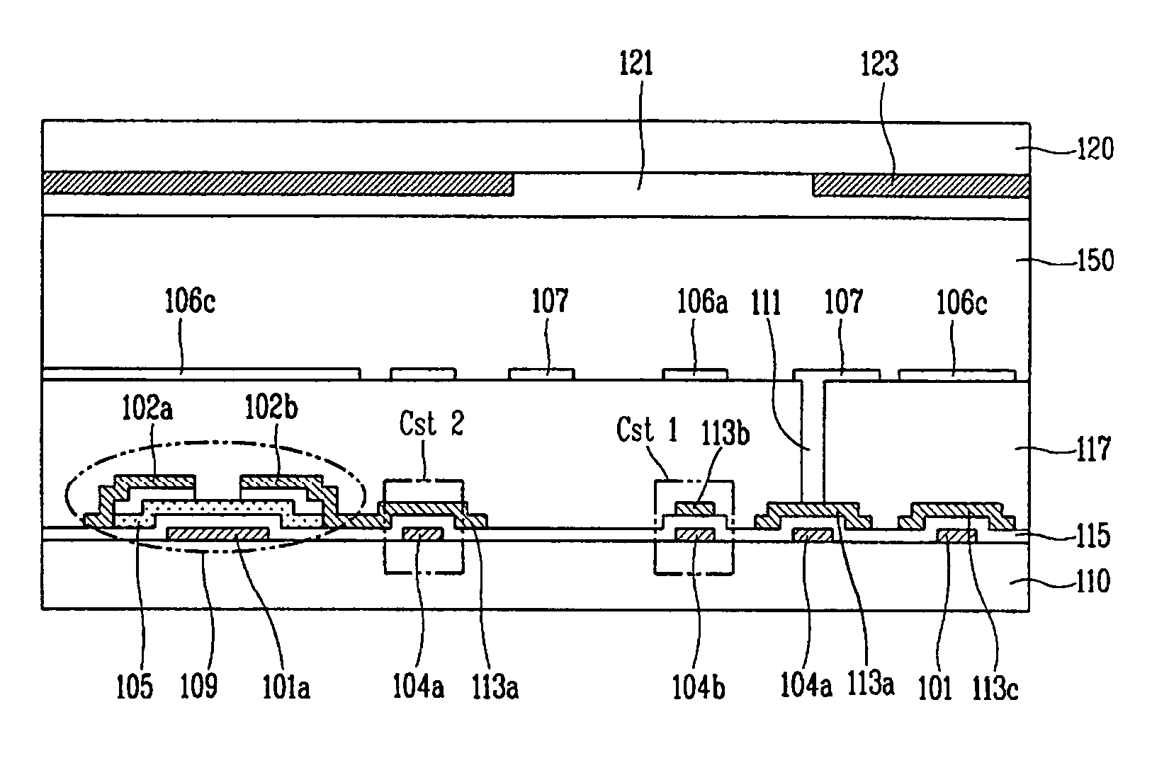
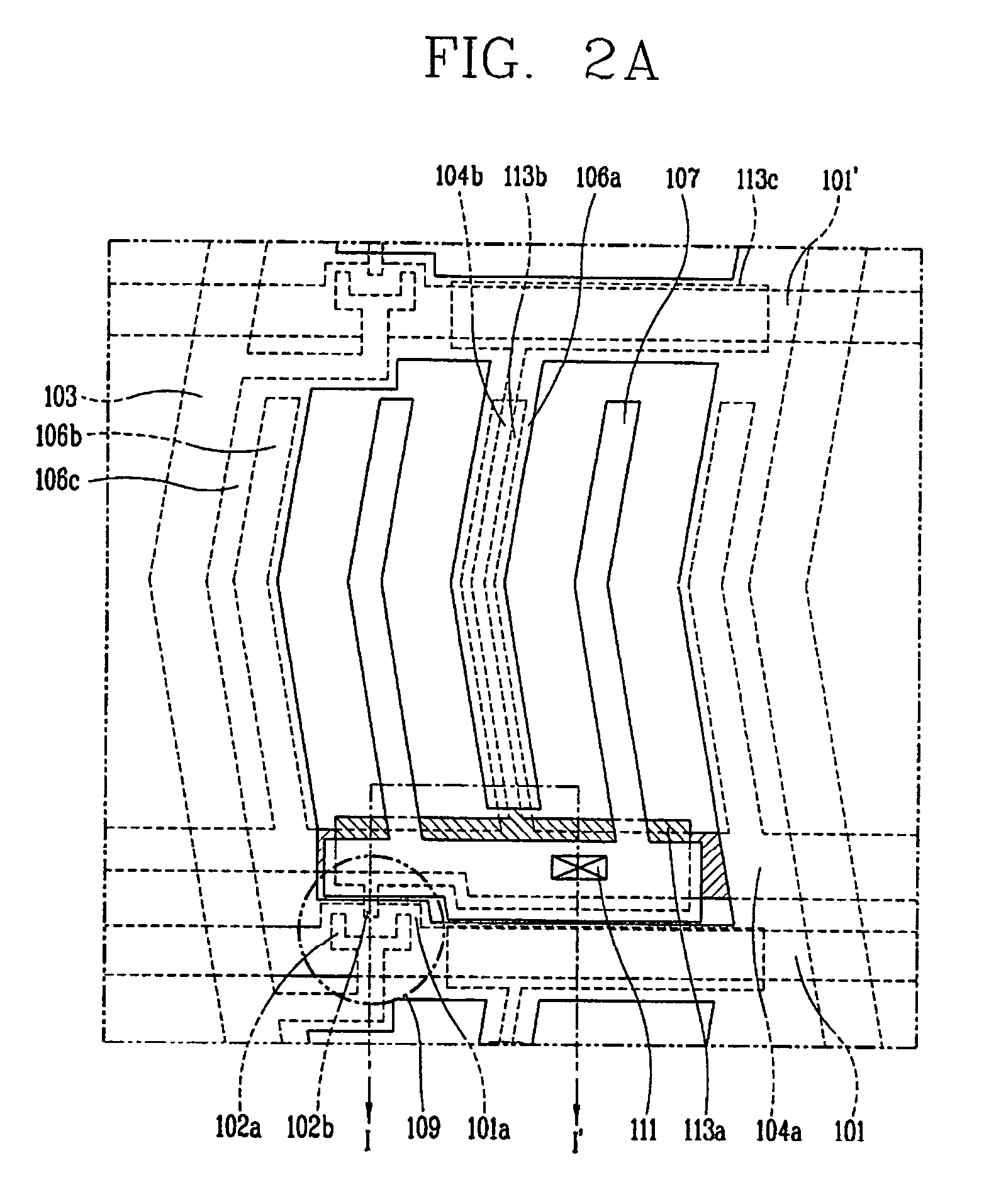
[0031]FIG. 2A is a plan view showing a unit pixel region of an IPS mode LCD device in accordance with the present invention, and FIG. 2B is a sectional view taken along line I-I′ of FIG. 2A.

[0032]As illustrated, a gate line 101 and a data line 103 are arranged horizontally and vertically on a first substrate 110 to define a pixel region, and at a crossing of the gate line 101 and the data line, there are formed a gate electrode 101a formed as a portion of the gate line 101, a semiconductor layer 105 formed on the gate electrode 101a and source and drain electrodes 102a and 102b disposed spaced apart from each other on the semiconductor layer 105 to form a switching device 109.

[0033]A passivation film 117 made of an organic insulation film with a low dielectric constant is deposited on the entire surface of the first substr...


PUM

PropertyMeasurementUnit
electric fieldaaaaaaaaaa
widthaaaaaaaaaa
transparentaaaaaaaaaa

Abstract

Disclosed is an in-plane switching (IPS) mode liquid crystal display (LCD) device having an increased aperture ratio by overlapping a storage capacitor on a lower end of an electrode. The (IPS) mode liquid crystal display device (LCD) device includes first and second substrates; a gate line and a data line arranged horizontally and vertically to define a plurality of pixel regions on the first substrate; a switching device, having a gate electrode, a semiconductor layer and source and drain electrodes, at a crossing of the gate line and the data line; a passivation film on an entire surface of the first substrate including the switching device; a common electrode and a pixel electrode alternately disposed at an upper portion of the passivation film and generating an in-plane electric field, wherein at least one of the common and pixel electrodes has a first storage capacitor at its lower end; and a liquid crystal layer between the first and second substrates.

Description

[0001]This application claims the benefit of Korean Patent Application No. 2004-105113, filed on Dec. 13, 2004, which is hereby incorporated by reference for all purposes as if fully set forth herein.BACKGROUND OF THE INVENTION[0002]1. Field of the Invention[0003]The present invention relates to a high aperture ratio liquid crystal display (LCD) device. More particularly, the present invention relates to an in-plane switching (IPS) mode LCD capable of enhancing an aperture ratio by forming a storage capacitor, namely, a light blocking region, to overlap with a lower end of at least one electrode.[0004]2. Description of the Related Art[0005]As the demand for various information display devices is increasing, research for a flat panel display device such as an LCD (Liquid Crystal Display), PDP (Plasma Display Panel), an ELD (Electro Luminescent Display), an FED (Field Emission Display) or a VFD (Vacuum Fluorescent Display) is actively ongoing. Of these displays, the LCD is the most sp...

Claims


Application Information

Patent Timeline
Patent Type & Authority Patents(United States)
IPC IPC(8): G02F1/1343
CPCG02F1/134363G02F1/136213G02F1/1343
Inventor PARK, SEUNG RYULLKIM, DONG GUK
Owner LG DISPLAY CO LTD
Why Eureka
Try Eureka