
Vertical thyristor in complementary SiGe bipolar process

a bipolar process and thyristor technology, applied in the field of thyristors, can solve the problems of low on-state resistance, high holding voltage, and process specifics that do not allow the formation of conventional lateral esd protection devices

Active Publication Date: 2009-04-21
NAT SEMICON CORP
View PDF2 Cites 4 Cited by
  • Summary
  • Abstract
  • Description
  • Claims
  • Application Information

AI Technical Summary

Problems solved by technology

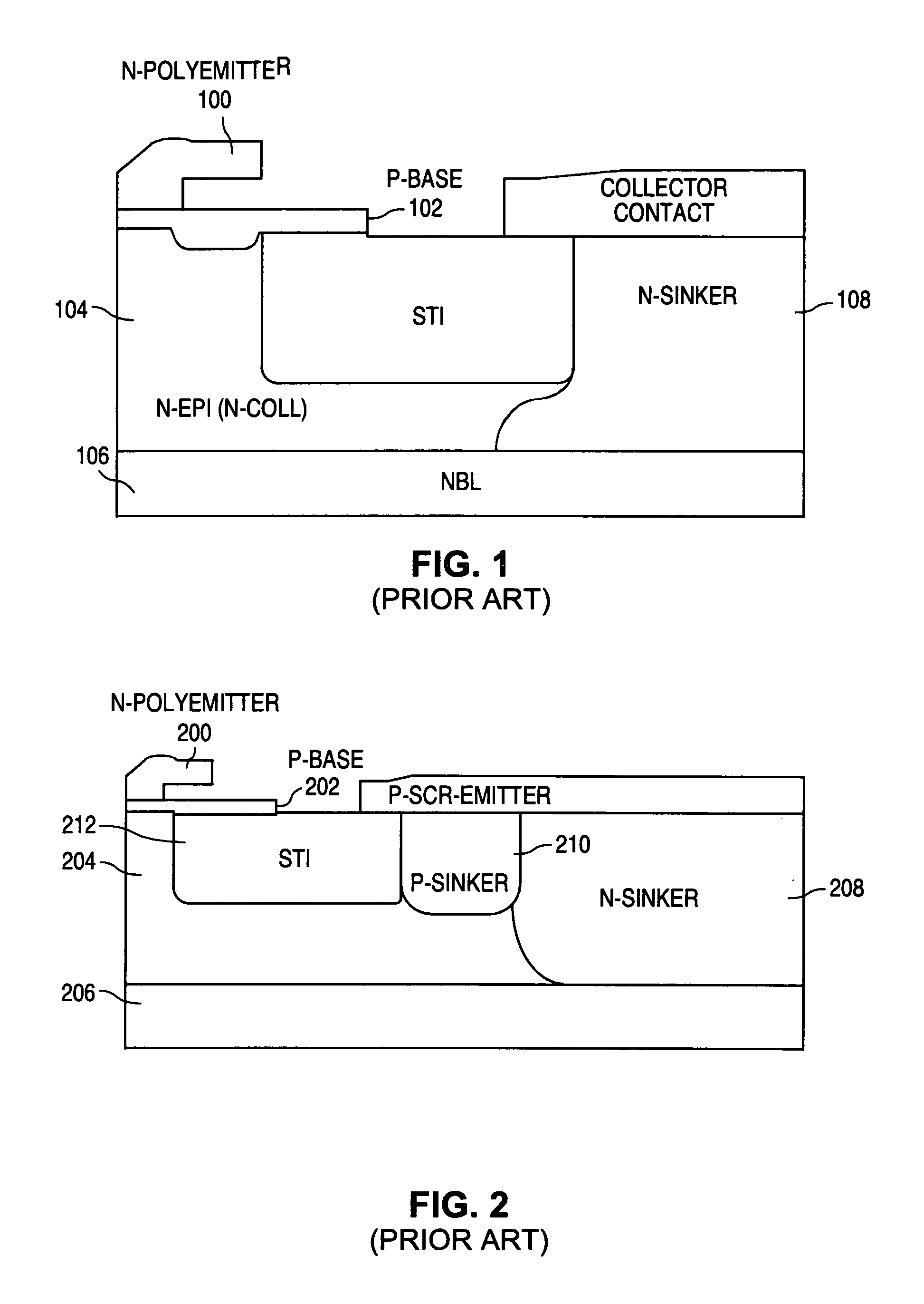
In complementary bipolar process the process specifics do not allow conventional lateral ESD protection devices to be formed.
Furthermore, difficulties are faced by bipolar junction devices as electrostatic discharge (ESD) protection structures, since in the case of high performance radio frequency bipolar junction transistors (RF BJTs) the subcollector is typically heavily doped which results in a high holding voltage and low on-state resistance due to the high density of injected carriers required after snapback.
SCRs as ESD protection structures also face difficulties in a bipolar process since in a vertical bipolar process the collector of an npn BJT is typically implemented using a subcollector comprising an n-buried layer.
This n-buried layer poses difficulties for SCR devices since it creates a high level of isolation of the p-emitter of the SCR.

Method used


Image

  • Vertical thyristor in complementary SiGe bipolar process
  • Vertical thyristor in complementary SiGe bipolar process
  • Vertical thyristor in complementary SiGe bipolar process

Examples


Embodiment Construction

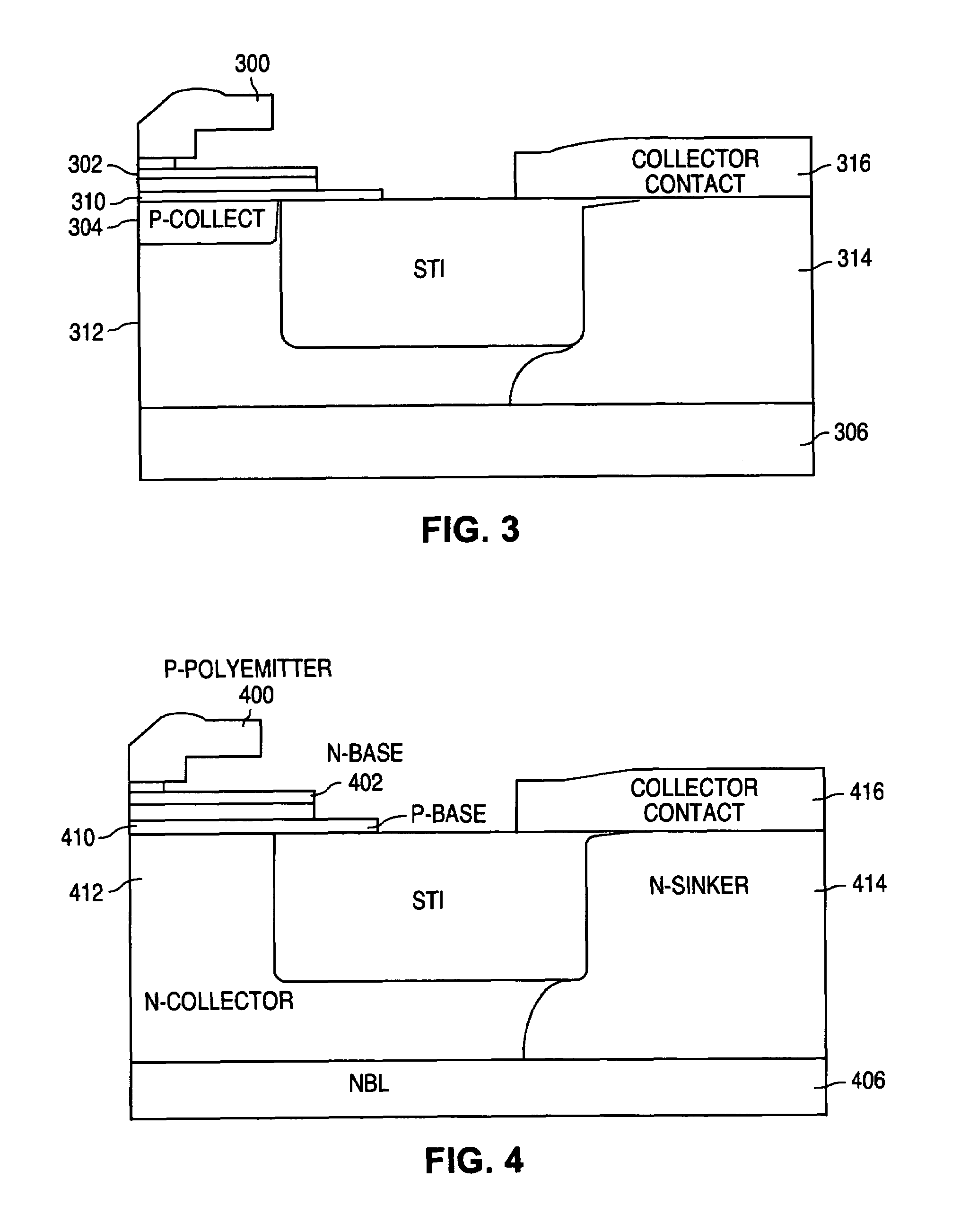
[0014]The present invention provides for a pnpn thyristor structure by making use of some of the layers provided in a complementary, SiGe base, bipolar process. For ease of discussion the various p and n layers used will be referred to with reference to their names as they would appear in bipolar structures and the invention will be described in terms of forming part of the bipolar transistors. One embodiment of a pnpn thyristor structure of the invention is shown in FIG. 3. This includes part of a vertical SiGe base pnp bipolar transistor formed on top of part of a vertical SiGe base npn bipolar transistor. In particular, as part of the process steps of forming an npn transistor, only the p-type SiGe base 310 and n-collector are used. The n-collector 312 extends into the subcollector comprising an n-buried layer (NBL) 306 and n-sinker 314 which connects to collector contact 316. The n-emitter of the npn transistor does not form part of the pnpn thyristor structure. The portions of ...


PUM


Abstract

In a complementary SiGe bipolar process, a pnpn thyristor structure is formed from some of the layers of a pnp transistor and an npn transistor formed on top of each other and making use of the SiGe gates to define the blocking junction.

Description

FIELD OF THE INVENTION[0001]The invention relates to thyristors and in particular to ESD devices formed in a complementary bipolar process.BACKGROUND OF THE INVENTION[0002]In complementary bipolar process the process specifics do not allow conventional lateral ESD protection devices to be formed.[0003]Furthermore, difficulties are faced by bipolar junction devices as electrostatic discharge (ESD) protection structures, since in the case of high performance radio frequency bipolar junction transistors (RF BJTs) the subcollector is typically heavily doped which results in a high holding voltage and low on-state resistance due to the high density of injected carriers required after snapback. Such a prior art vertical BJT is shown in cross section in FIG. 1, which shows an n-polysilicon emitter 100 formed on a p-base 102 and an n-epitaxially grown collector 104 with subcollector in the form of an n-buried layer (NBL) 106 contacted through an n-sinker 108.[0004]SCRs as ESD protection str...

Claims


Application Information

Patent Timeline
IPC IPC(8): H01L21/8238
CPCH01L21/8222H01L27/0641H01L27/0817
Inventor VASHCHENKO, VLADISLAVSADOVNIKOV, ALEXELHOPPER, PETER J.
Owner NAT SEMICON CORP
Learn More