Three-dimensional integrated semiconductor devices

a semiconductor device and three-dimensional technology, applied in the field of three-dimensional integrated semiconductor devices, can solve the problems of increasing the functional density, interconnecting, and limiting the chip area, and improving the circuit performan

Inactive Publication Date: 2005-09-13
ADVANCED MICRO DEVICES INC
View PDF14 Cites 517 Cited by
  • Summary
  • Abstract
  • Description
  • Claims
  • Application Information

AI Technical Summary

Problems solved by technology

However, the area which is occupied by the interconnection lines between the on-chip devices grew more quickly, as exemplified below, such that the condition was reached in which the functional density, and therefore the chip area, became interconnect-limited.
This means that the shrinking of device structures does not lead to an increase in functional density, and would, therefore, not lead to an improved circuit performance.
Consequently, there exists a limitation point where an additional device element would require as much additional area of interconnection lines that the functional density would decrease although the structure size decreases.
With regard to improvement in circuit performance by increasing circuit speed, there are also limitations due to the switching speed of MOS transistors and the propagation delay in the interconnect wires.
In other words, as the devices shrink, the device contribution to the propagation delay also decreases.
Scaling down interconnection line widths, however, necessarily increases the propagation delay time due to the increasing resistance and parasit

Method used


Image

  • Three-dimensional integrated semiconductor devices
  • Three-dimensional integrated semiconductor devices
  • Three-dimensional integrated semiconductor devices

Examples


Embodiment Construction

[0034]Illustrative embodiments of the invention are described below. In the interest of clarity, not all features of an actual implementation are described in this specification. It will of course be appreciated that in the development of any such actual embodiment, numerous implementation-specific decisions must be made to achieve the developers' specific goals, such as compliance with system-related and business-related constraints, which will vary from one implementation to another. Moreover, it will be appreciated that such a development effort might be complex and time-consuming, but would nevertheless be a routine undertaking for those of ordinary skill in the art having the benefit of this disclosure.

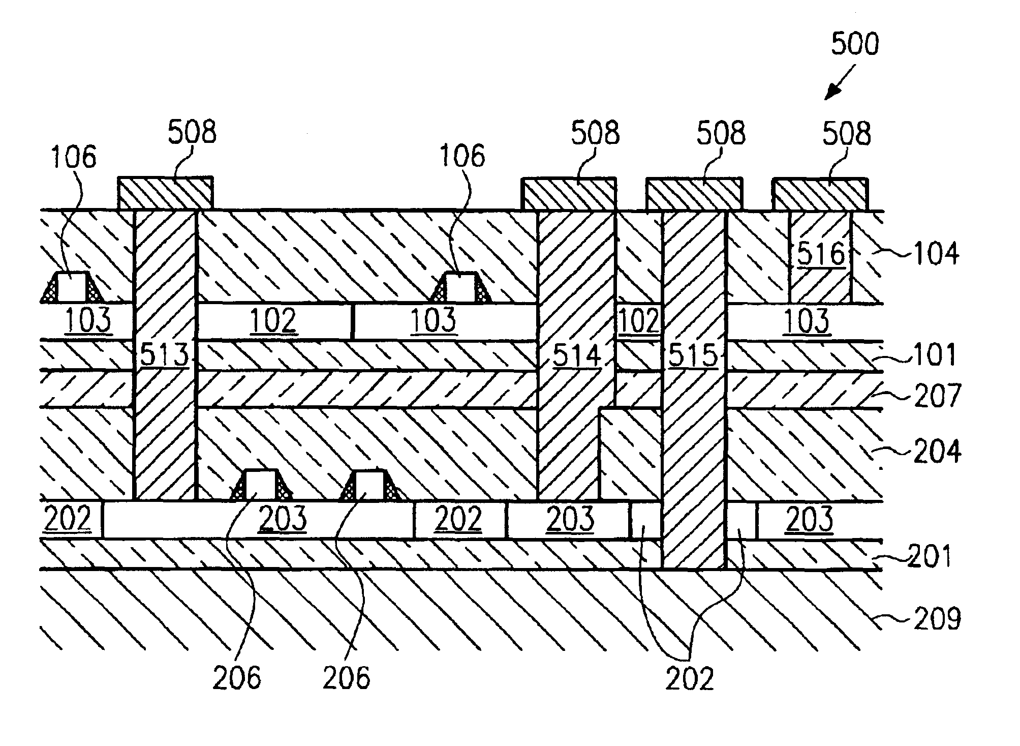
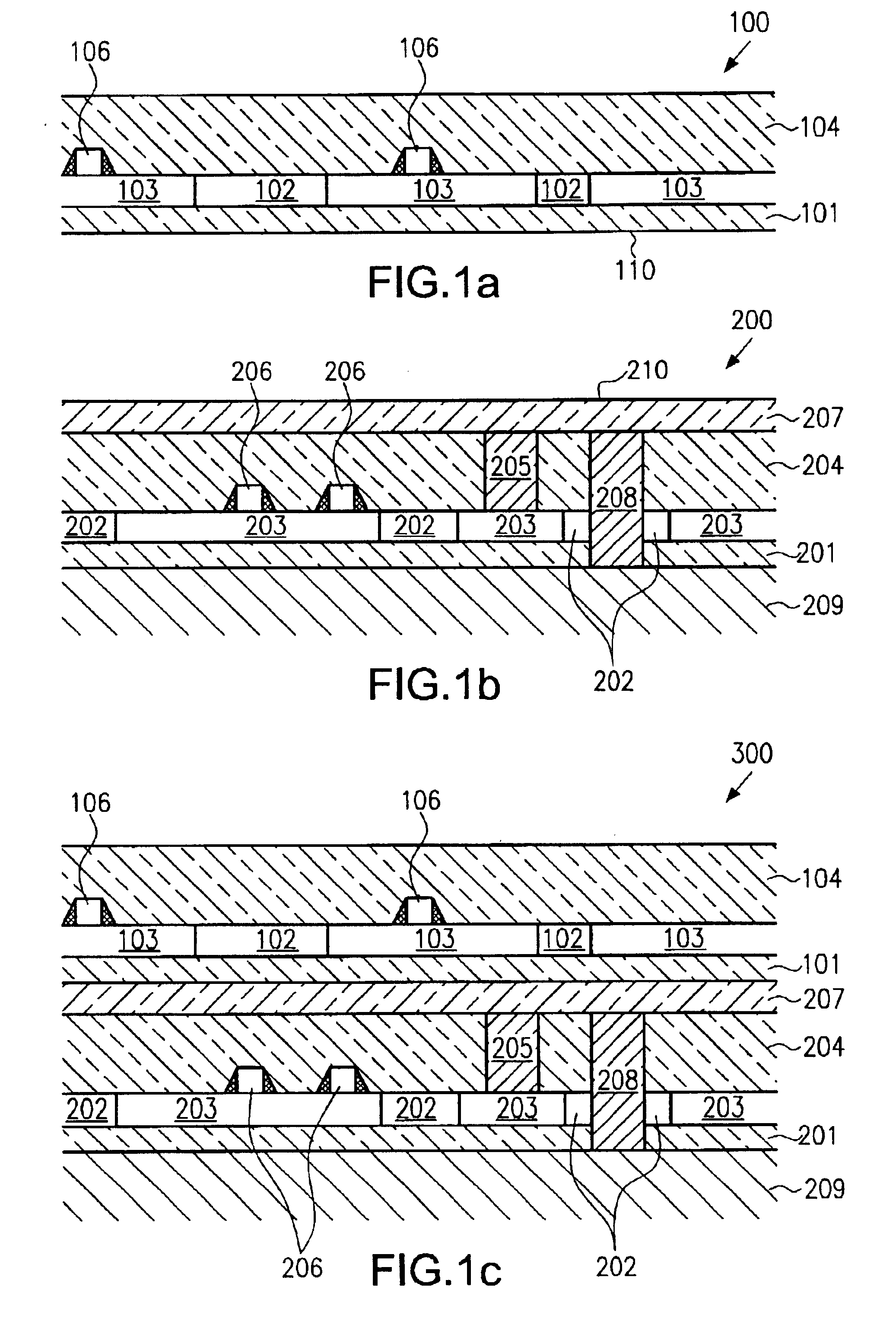
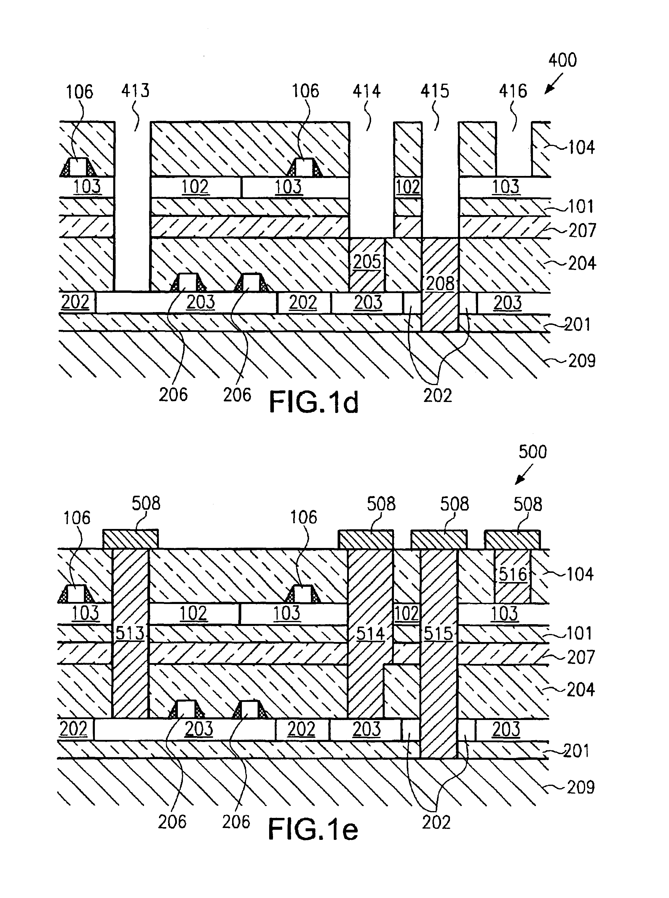
[0035]The present invention describes a process for three-dimensional integration of semiconductor devices and a resulting device. The process combines low temperature wafer bonding methods with backside / substrate contact processing methods, preferably with silicon on insulator d...


PUM


Abstract

The present invention describes a process for three-dimensional integration of semiconductor devices and a resulting device. The process combines low temperature wafer bonding methods with backside/substrate contact processing methods, preferably with silicon on insulator devices. The present invention utilizes, in an inventive fashion, low temperature bonding processes used for bonded silicon on insulator (SOI) wafer technology. This low temperature bonding technology is adopted for stacking several silicon layers on top of each other and building active transistors and other circuit elements in each one. The back-side/substrate contact processing methods allow the interconnection of the bonded SOI layers.

Description

BACKGROUND OF THE INVENTION[0001]1. Field of the Invention[0002]The present invention relates to the field of fabrication of integrated circuits, and, more particularly, to semiconductor structures wherein integrated circuits are stacked on top of each other to allow vertically integrated circuits.[0003]2. Description of the Related Art[0004]Throughout the evolution of integrated circuits, it has been realized that the need for improvements can be focused on two items: (1) increasing the functional complexity of the circuits, whereby the device area should decrease; and (2) increasing the circuit speed, allowing an overall improvement of the circuit performance. With regard to the increase in functional complexity, this results mainly in an increase in functional density, while at the same time the shrinking size of chip structures is also of importance. The functional density, which is of primary importance, is defined as the number of interconnected devices per chip area. In contr...

Claims


Application Information

Patent Timeline
IPC IPC(8): H01L21/70H01L23/48H01L21/822H01L21/768H01L27/06H01L27/12H01L21/84H01L25/065
CPCH01L21/743H01L21/76898H01L21/8221H01L21/84H01L23/481H01L25/50H01L27/0688H01L27/1203H01L25/0657H01L2924/0002H01L2924/00
Inventor GREENLAW, DAVID
Owner ADVANCED MICRO DEVICES INC
Why Eureka
Try Eureka