Dielectric wafer level bonding with conductive feed-throughs for electrical connection and thermal management

a technology of dielectric wafers and feed-throughs, applied in the field of electrical connection and thermal management of dielectric wafers, can solve the problems of limiting device performance, limiting optical applications, and generally more expensive materials, and achieve the effect of increasing the number of device types accessibl

Active Publication Date: 2007-12-13
CREELED INC
View PDF22 Cites 68 Cited by
  • Summary
  • Abstract
  • Description
  • Claims
  • Application Information

AI Technical Summary

Benefits of technology

[0013] Briefly, and in general terms, the present invention is directed to wafer bonded devices and wafer level bonding methods which increase the number of device types accessible to wafer bonding w...

Problems solved by technology

However, Si's limited bandgap and its modest mobilities can limit device performance and restrict optical applications.
Alternatively, gallium arsenide (GaAs) and other compound semiconductors with better bandgap characteristics or mobilities can also be used, but such materials are generally more costly.
However, wafer bonding with eutectic materials is currently limited to vertical device geometries where the second electrical contact is provided by a wire bond to the top of the chip.
Also, selective area wafer alignment bonding...

Method used


Image

  • Dielectric wafer level bonding with conductive feed-throughs for electrical connection and thermal management
  • Dielectric wafer level bonding with conductive feed-throughs for electrical connection and thermal management
  • Dielectric wafer level bonding with conductive feed-throughs for electrical connection and thermal management

Examples


Embodiment Construction

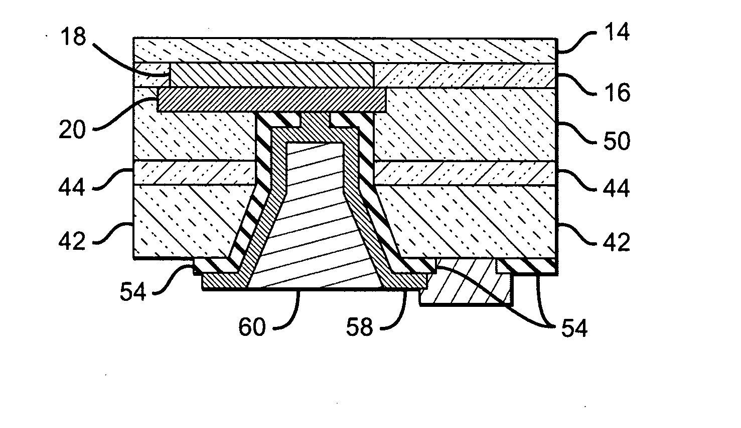
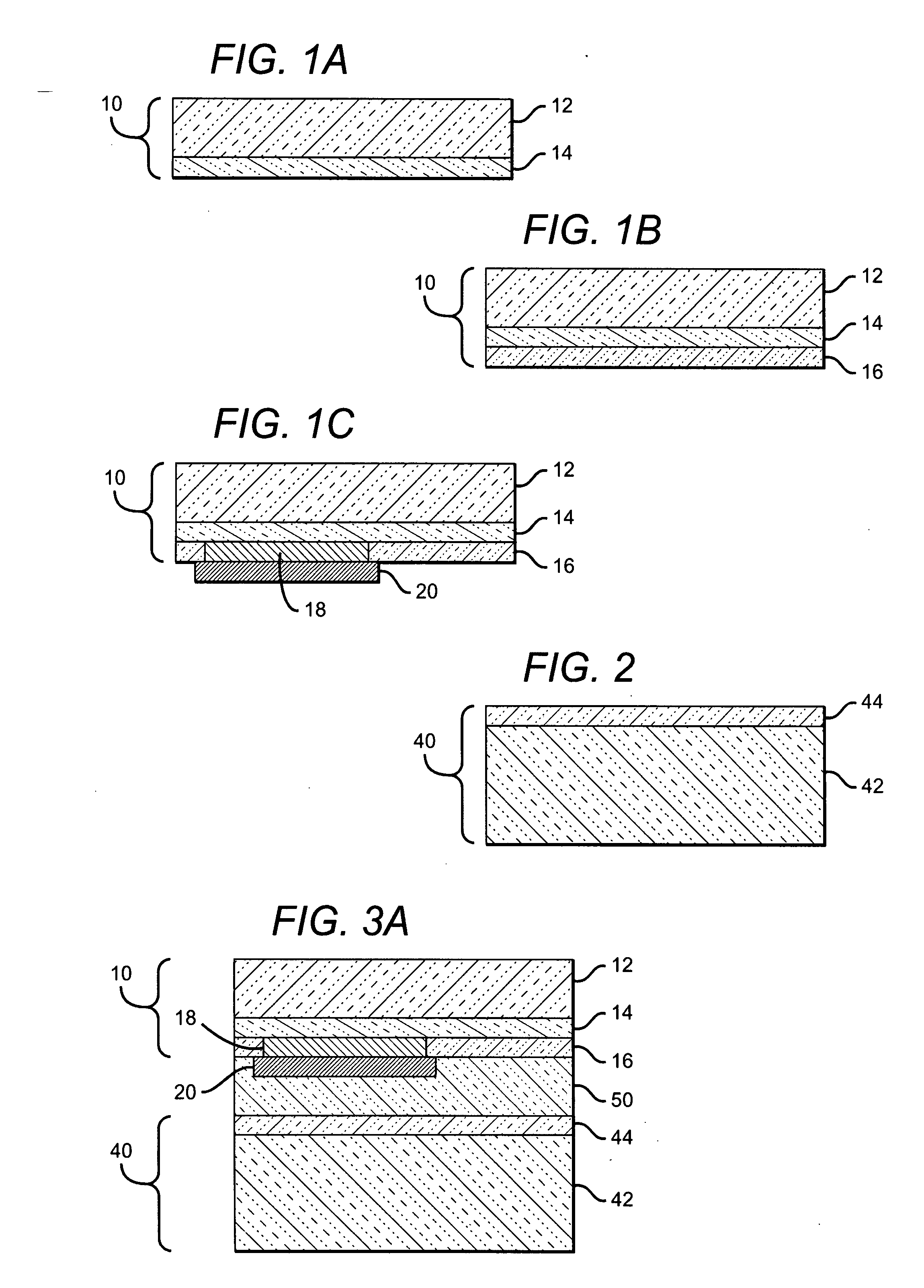
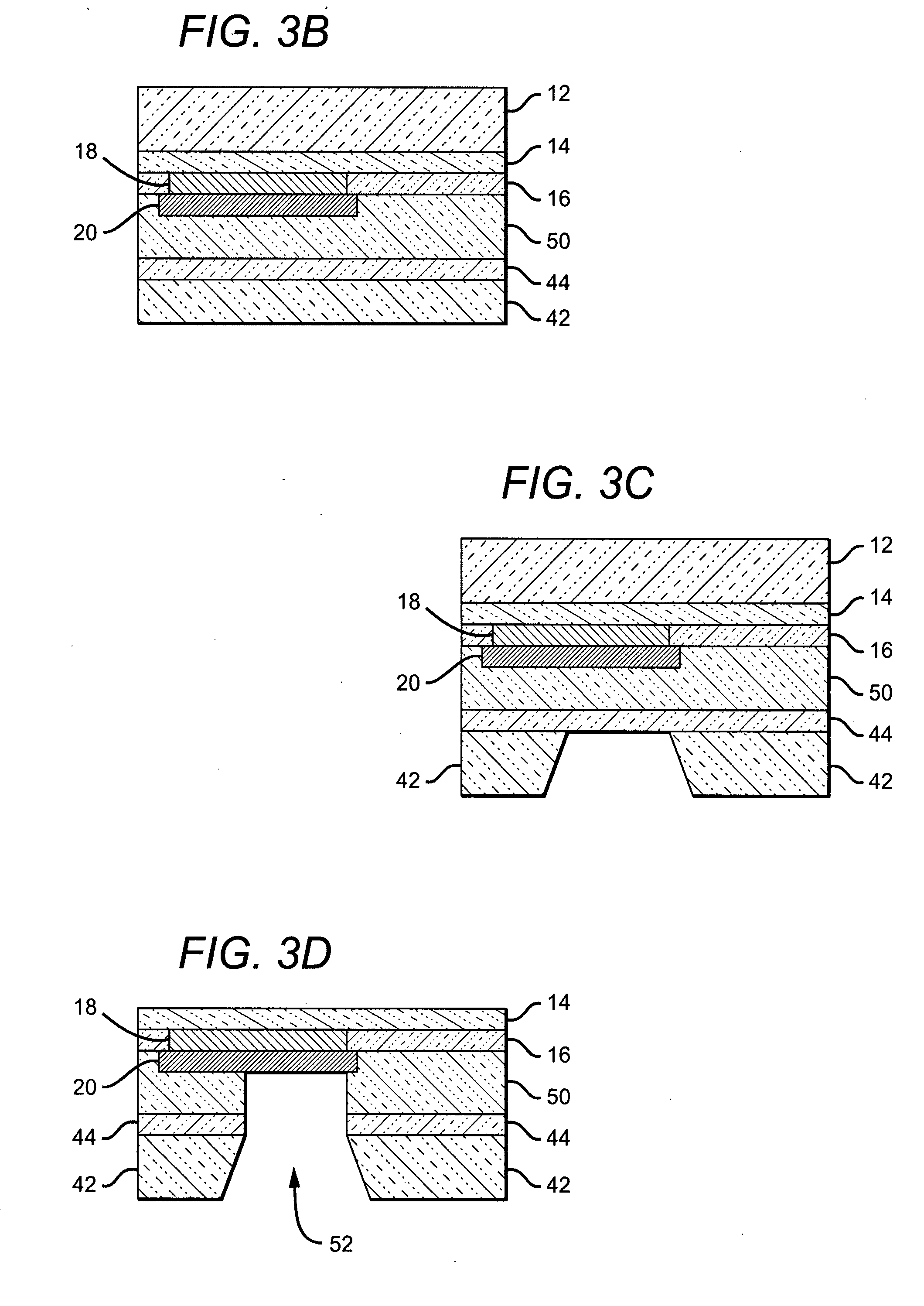
[0024] The present invention relates to the devices such as light emitting devices (LEDs) where most of the processing steps occur at the wafer level, thereby reducing overall fabrication costs. The resulting LEDs can also be contacted from the backside, making packaging of the LED easier with the LEDs requiring less packaging space and material.

[0025] In particular, the invention relates to the use of electrically insulating, dielectric medium for wafer bonding. In particular the invention introduces a thermally and electrically insulating material at the wafer level without using electro-thermally conducting bond medium. To improve the thermal properties of the finished device, and to provide two electrical contacts to the LED from the bottom of the submount wafer, vias can be fabricated into the submount wafer and bonding medium after the wafer bonding process (post bond). The vias may subsequently be filled with thermally conductive material to improve the thermal properties of...


PUM


Abstract

A method for fabricating semiconductor and electronic devices at the wafer level is described. In this method, dielectric material is used to wafer bond a device wafer to a submount wafer, after which vias can be structured into the submount wafer and dielectric bonding material to access contact pads on the bonded surface of the device wafer. The vias may subsequently be filled with electrically and thermally conducting material to provide electrical contacts to the device and improve the thermal properties of the finished device, respectively. The post-bonding process described provides a simple, cost-effective, non-alignment method for fabricating a variety of electronic and semiconductor devices, particularly light emitting diodes with electrical contacts at the bottom of the chip.

Description

RELATED APPLICATION DATA [0001] This application is a continuation-in-part of U.S. application Ser. No. 10 / 171,893 which claims the benefit of U.S Provisional patent application Ser. No. 60 / 584,187 filed Jun. 30, 2004.STATEMENT AS TO FEDERALLY SPONSORED RESEARCH [0002] This invention was made with Government support under contract no. 70NANB4H3037 awarded by the Department of Commerce. The federal government may have certain rights in the invention.BACKGROUND OF THE INVENTION [0003] 1. Field of the Invention [0004] The present invention relates to electronic and semiconductor devices, and more particularly to light emitting devices and methods of fabricating light emitting devices. [0005] 2. Description of Related Art [0006] Light emitting diodes and laser diodes are well known solid state electronic devices capable of generating light upon application of a sufficient voltage. Light emitting diodes and laser diodes may be generally referred to as light emitting devices (LEDs). Light...

Claims


Application Information

Patent Timeline
IPC IPC(8): H01L33/00H01L21/30H01L23/52H01L33/38
CPCH01L23/481H01L33/0079H01L33/382H01L33/64H01L33/647H01L2924/0002H01L2924/3011H01L2924/00H01L33/0093
Inventor CHITNIS, ASHAYIBBETSON, JAMES
Owner CREELED INC
Why Eureka
Try Eureka