Semiconductor device having through electrode and method of manufacturing the same

a technology of through electrode and semiconductor device, which is applied in the direction of semiconductor device, semiconductor/solid-state device details, electrical apparatus, etc., can solve the problem of limiting the size reduction, and achieve the effect of reducing the size, reducing the cost, and increasing the density

a technology of through electrode and semiconductor device, which is applied in the direction of semiconductor device, semiconductor/solid-state device details, electrical apparatus, etc., can solve the problem of limiting the size reduction, and achieve the effect of reducing the size, reducing the cost, and increasing the density

US7524753B2Active Publication Date: 2009-04-28SHINKO ELECTRIC IND CO LTD

Image

  • Semiconductor device having through electrode and method of manufacturing the same
  • Semiconductor device having through electrode and method of manufacturing the same
  • Semiconductor device having through electrode and method of manufacturing the same

Examples


Embodiment Construction

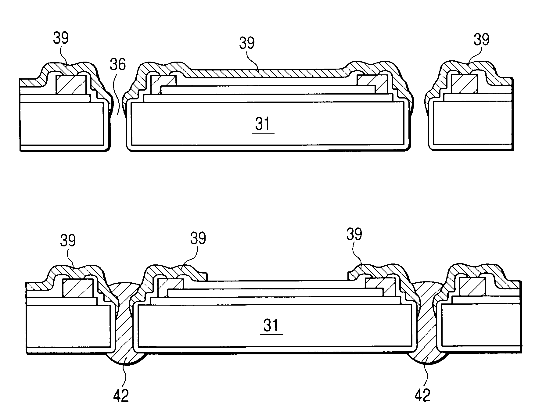
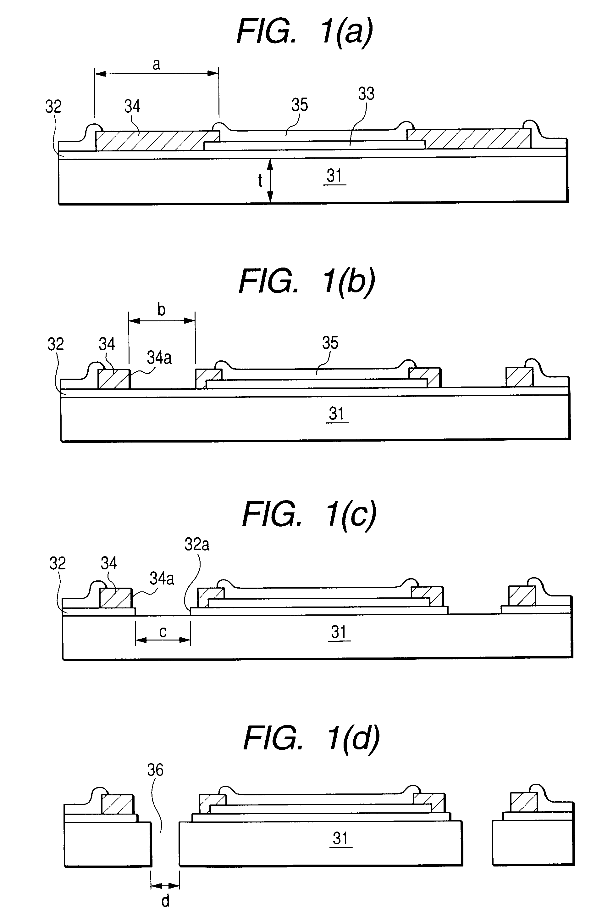
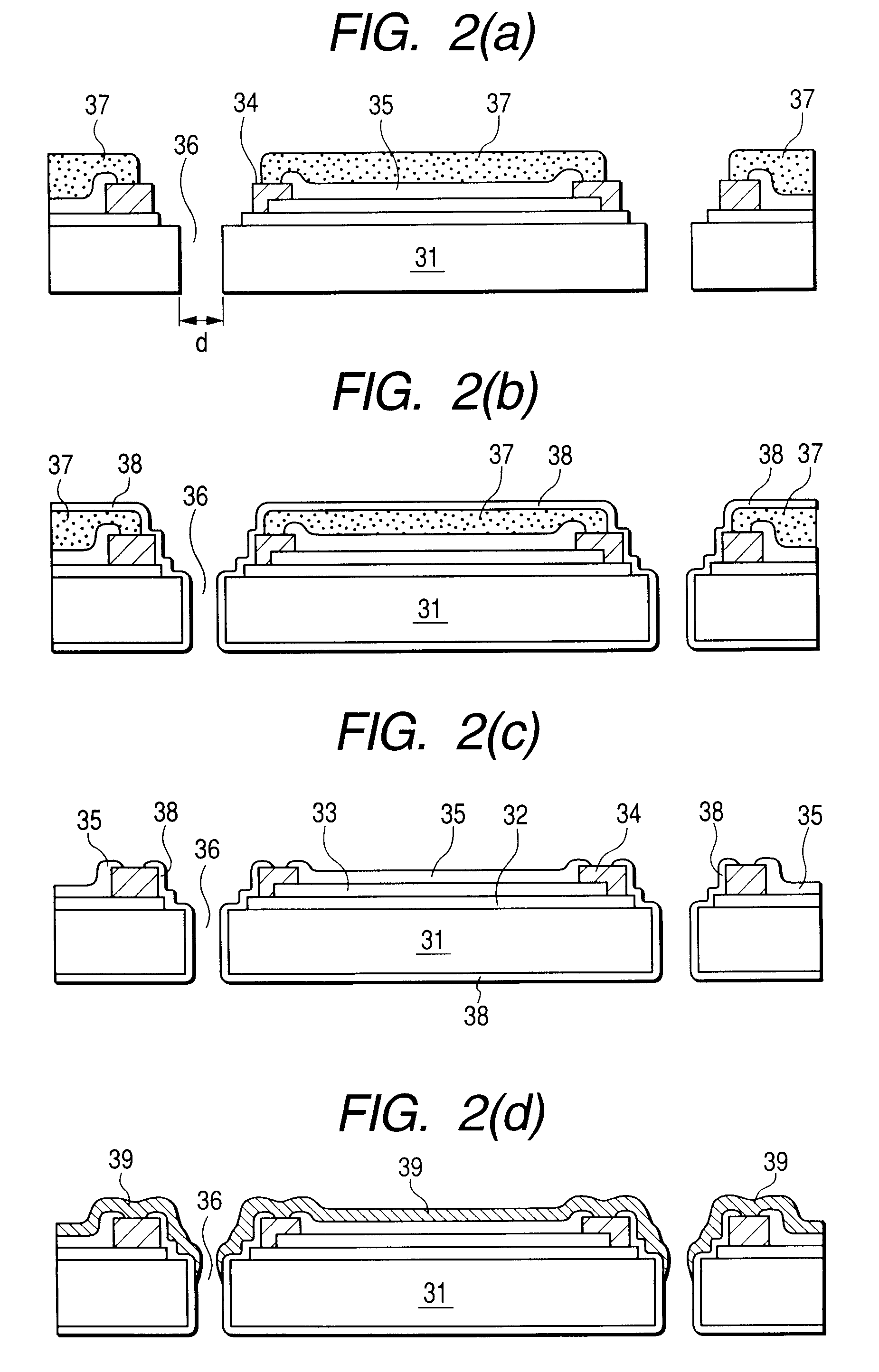
[0025]An embodiment of the present invention will be explained in detail with reference to FIG. 1 toFIG. 4 hereinafter. FIGS. 1(a) to (d), FIGS. 2(a) to (d), and FIGS. 3(a) to (d) show a method of manufacturing a semiconductor device having a through electrode of the present invention in order of step.

[0026]FIG. 1(a) shows a semiconductor wafer (wiring substrate) In this semiconductor wafer, an oxide film (SiO2 film) 32 is formed as an insulating film that covers an upper surface of a silicon (Si) substrate (semiconductor substrate) 31. Then, a device layer 33 such as a CCD or CMOS image sensor, a memory, or the like is formed on the oxide film 32. Then, aluminum pads (electrode pads) 34 are formed around the device layer 33 on the oxide film 32 such that a part of them is overlapped with the device layer 33. Then, an insulating film (passivating film) 35 is formed thereon over a whole surface. Then, only the passivating film 35 located on the aluminum pads 34 is removed from areas ...


PUM

PropertyMeasurementUnit
lengthaaaaaaaaaa
thicknessaaaaaaaaaa
lengthaaaaaaaaaa

Abstract

A method of manufacturing a semiconductor device having a through electrode, includes forming through holes 36 in a substrate 31, forming a first metal layer 39 from one surface side of the substrate and pasting a protection film 40 on one surface of the substrate, forming through electrodes by filling the through holes with a second metal by means of an electroplating of the second metal 42 applied from other surface of the substrate while using the first metal layer as a power feeding layer, removing the protection film 40, and removing the first metal layer 39 located in areas other than peripheral portions of the through electrodes.

Description

TECHNICAL FIELD[0001]The present disclosure relates to a semiconductor device having a through electrode and a method of manufacturing the semiconductor device having the through electrode. The present disclosure can be applied as a three-dimensional packaging method, for example, that is applied to form through electrodes in a silicon substrate, in devices such as a CCD (charge coupled device) for receiving a light converged by a condensing lens, a CMOS device, a memory device, and the like and module parts such as a camera module, a memory multi-stage module, and the like.RELATED ART[0002]With the rapid progress and development of the information communication technology, improvement in a data communication speed and increase of an amount of data communication can be realized recently. Among the mobile electronic devices such as the cellular phone, the notebook personal computer, and the like, the mobile electronic device into which the imaging device having the image pickup devic...

Claims


Application Information

Patent Timeline
28 Apr 2009
Publication
US7524753B2
IPC
H01L21/44; H01L29/40
CPC
H01L21/76898; H01L23/481; H01L2224/16; H01L2224/48091; H01L2224/48227; H01L2224/73265; H01L2924/01077; H01L2924/01078
Inventors
SUNOHARA, MASAHIRO; HIGASHI, MITSUTOSHI