

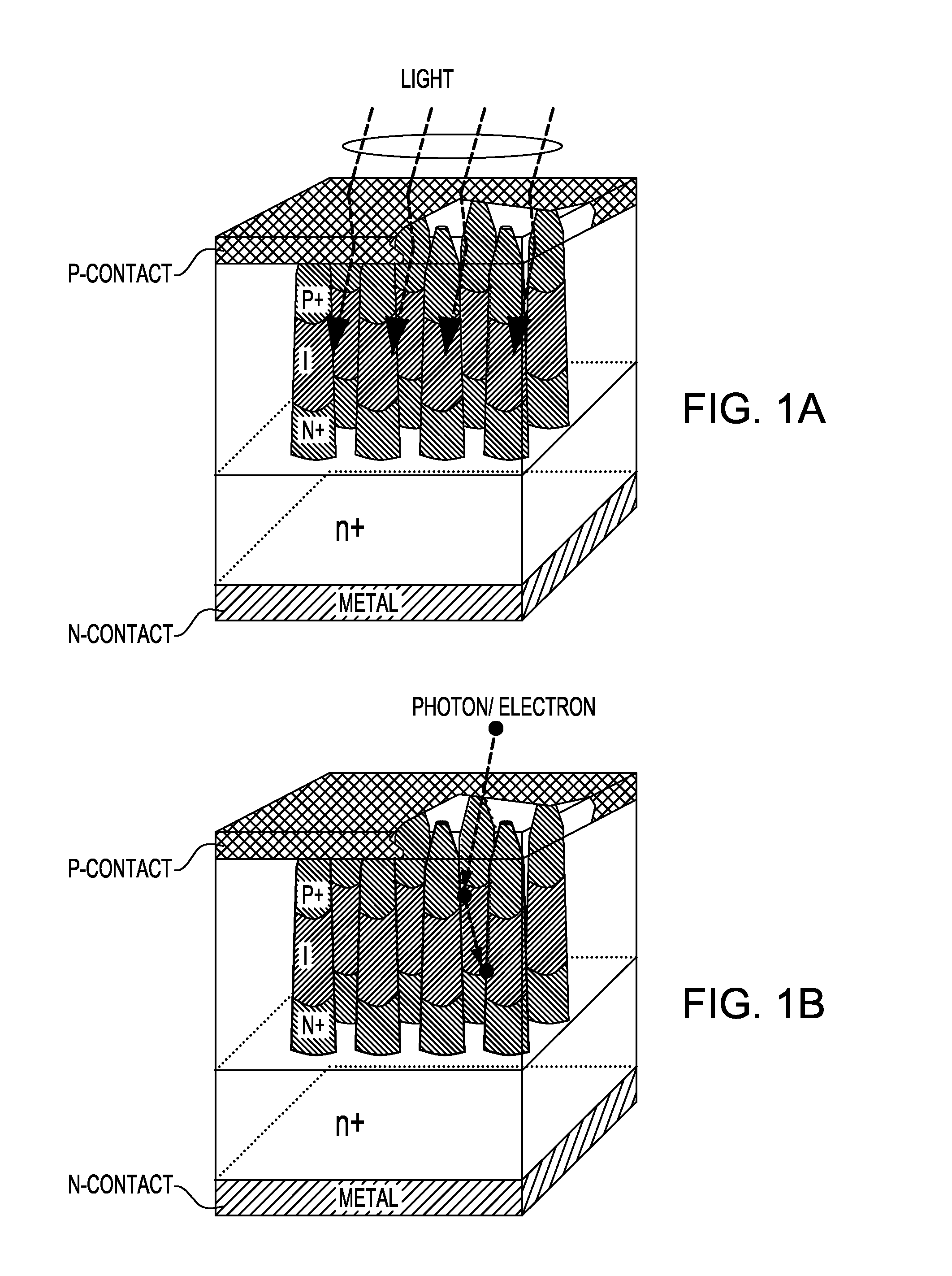
Pillar P-i-n semiconductor diodes
a technology of semiconductor diodes and pin diodes, which is applied in the field of integrated semiconductor pillar pin diodes, can solve the problems of limiting the sensitivity and/or the response of silicon p-i-n diodes, adversely affecting the area density of the device, and the majority of the photons that impinge on the planar surface of the device are reflected and lost, so as to maximize the number of photons impinging, improve the reliability of the device, and improve the effect of performan
- Summary
- Abstract
- Description
- Claims
- Application Information
AI Technical Summary
Benefits of technology
Problems solved by technology
Method used
Image

Examples
first embodiment
[0034]the fabrication steps to manufacture p-i-n diodes is described in FIGS. 3A-3G in which like numerals represent the same or similar elements.
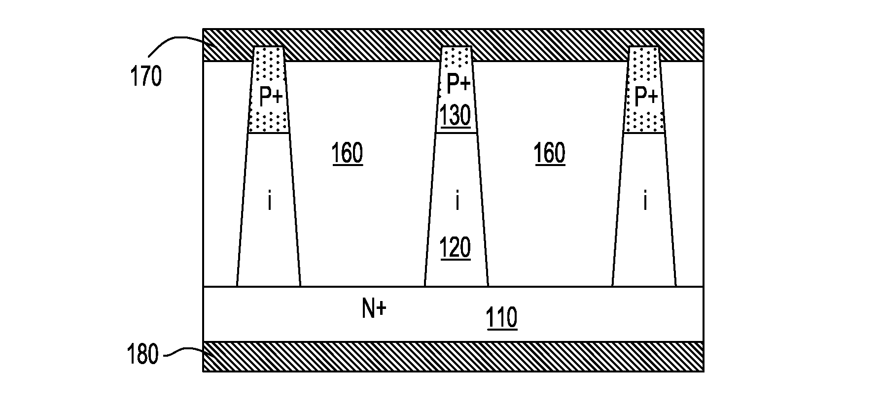
[0035]Referring to FIG. 3A, a semiconductor substrate 100 preferably made of silicon is provided. An N+ layer 110 is formed on a surface of the substrate. The N+ layer 110 contains N-type dopants such as phosphorus, arsenic, antimony, sulfur, selenium, and the like. The process of forming the N+ layer includes but is not limited to ion implantation, plasma doping, plasma immersion ion implantation, infusion doping, gas phase doping, in-situ doped epitaxial growth, solid phase doping (by depositing a dopant source layer such as arsenic-doped oxide, driving dopants into the substrate by high-temperature anneal, and removing the dopant source layer), and any combination thereof. Alternatively, the entire substrate is doped.
[0036]Referring to FIG. 3B, an intrinsic or lightly doped layer (i-layer) 120 is epitaxially grown on the N+ layer 110. A...
third embodiment
[0049]fabricating p-i-n diodes is described in FIG. 5A to FIG. 5H. In this embodiment, the N+ region is formed after forming silicon pillars so that the N+ region is self-aligned to the pillars.
[0050]Referring to FIG. 5A, an intrinsic or lightly doped semiconductor substrate such as silicon is provided. Referring to FIG. 5B, silicon pillars 310 are formed by patterning a mask layer 320 and then transferring the patterns in the mask layer 320 into the substrate 300.
[0051]Referring to FIG. 5C, spacers 330 are formed on the pillar sidewalls. Preferably, the spacer is made of silicon nitride. Alternatively, silicon oxide may be advantageously used.
[0052]Referring to FIG. 5D, an N+ region 340 self-aligned to pillars 310 is formed in the substrate. Processes for forming the N+ layer include, but are not limited to ion implantation, plasma doping, plasma immersion ion implantation, infusion doping, gas phase doping, in-situ doped epitaxial growth, solid phase doping (by depositing a dopant...
PUM
 Abstract
Description
Claims
Application Information