

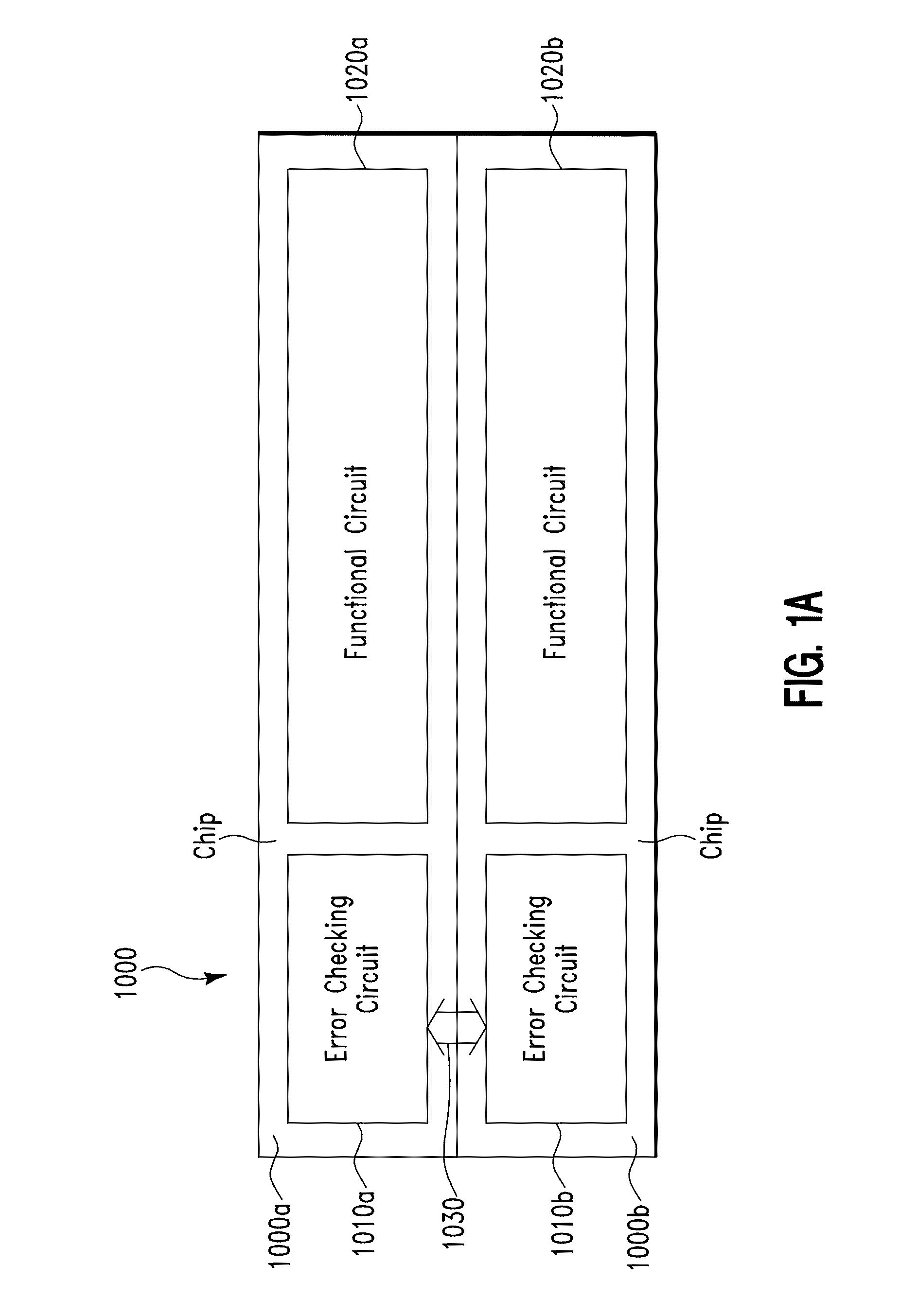
Error detection and correction in semiconductor structures
a technology of semiconductor structure and error detection, applied in the field of semiconductor structure error detection and correction, can solve the problem of limited number of signals that can be compared (checked)
- Summary
- Abstract
- Description
- Claims
- Application Information
AI Technical Summary
Benefits of technology
Problems solved by technology
Method used
Image

Examples
first embodiment
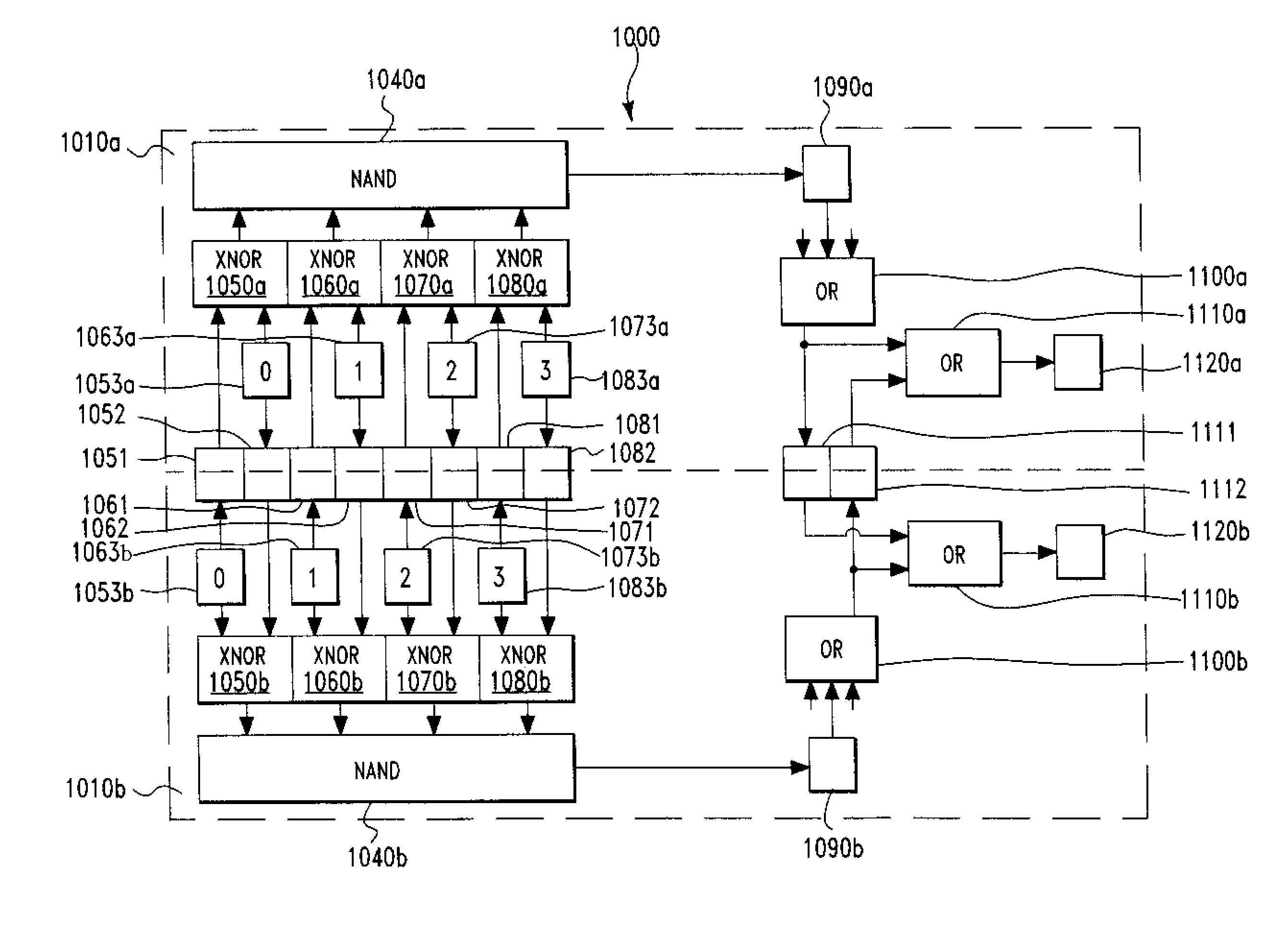
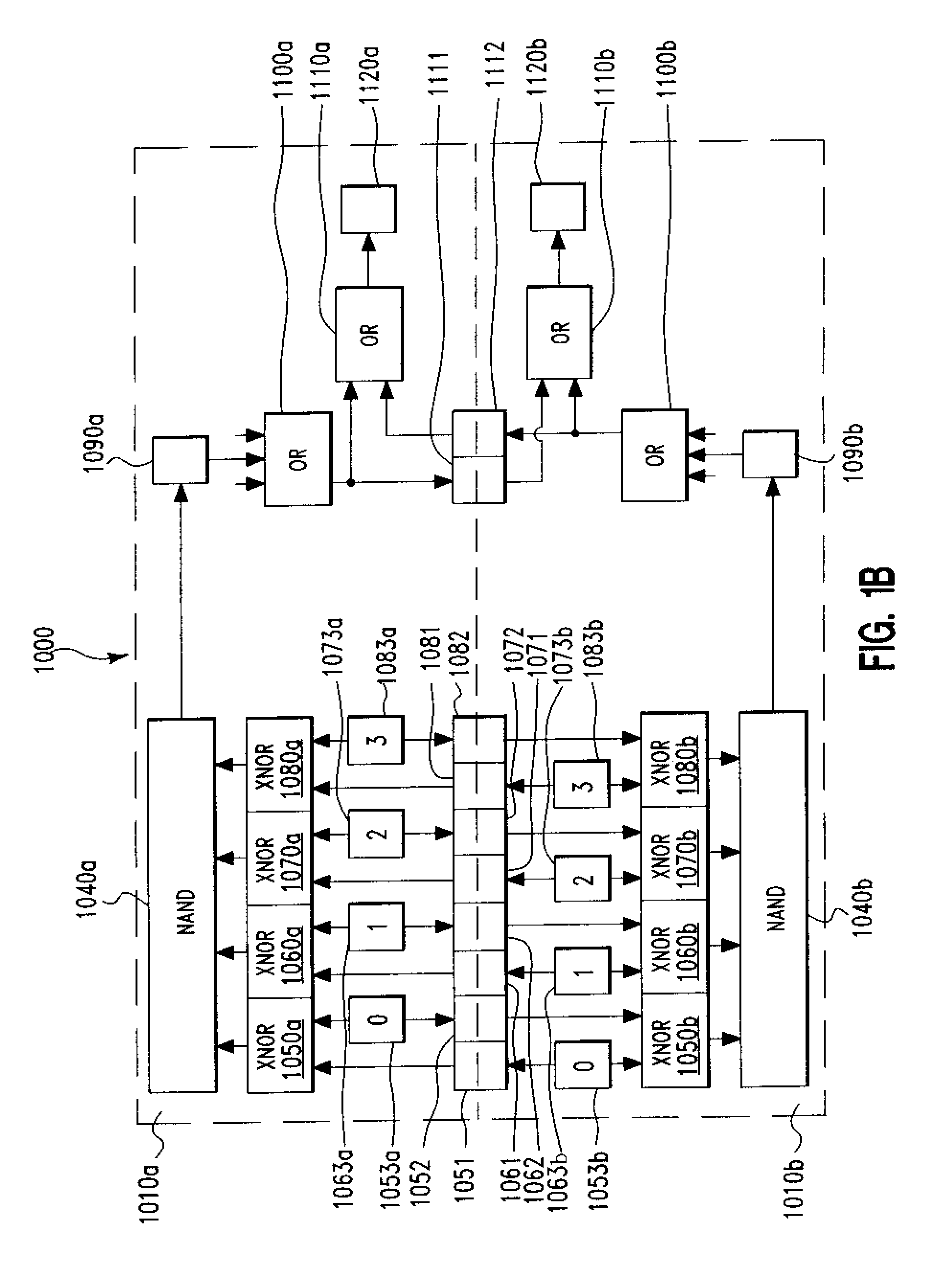
[0014]FIG. 1B illustrates the first and second error checking circuits 1010a and 1010b and the coupling vias 1030 of FIG. 1A. In one embodiment, more specifically, the first error checking circuit 1010a comprises a first NAND circuit 1040a, four exclusive-NOR circuits 1050a, 1060a, 1070a and 1080a, two OR circuits 1100a and 1110a, a first local error latch 1090a, and a first master error latch 1120a. Similarly, in one embodiment, the second error checking circuit 1010b comprises a second NAND circuit 1040b, four exclusive-NOR circuits 1050b, 1060b, 1070b and 1080b, two OR circuits 1100b and 1110b, a second local error latch 1090b and a second master error latch 1120b. The first and second error checking circuits 1010a and 1010b are used to identify any mismatch between any pair of four functional latches pairs 1053a and 1053b, 1063a and 1063b, 1073a and 1073b, 1083a and 1083b. In one embodiment, the coupling vias 1030 comprise ten coupling vias 1051, 1052, 1061, 1062, 1071, 1072, 10...
second embodiment
[0018]FIG. 1C illustrates the first and second error checking circuits 1010a and 1010b and the coupling vias 1030 of FIG. 1A. In one embodiment, more specifically, the first error checking circuit 1010a comprises a first NAND circuit 1130a, two exclusive-NOR circuits 1140 and 1150, three OR circuits 1160a, 1180a and 1190a, a first local error latch 1170a and a first master error latch 1200a. Similarly, in one embodiment, the second error checking circuit 1010b comprises a second NAND circuit 1130b, two exclusive-NOR circuits 1210 and 1220, three OR circuits 1160b, 1180b and 1190b, a second local error latch 1170b and a second master error latch 1200b. The first and second error checking circuits 1010a and 1010b are used to identify any mismatch between any pair of four functional latches pairs 1141a and 1141b, 1151a and 1151b, 1211a and 1211b, 1221a and 1221b. In one embodiment, the coupling vias 1030 comprise eight coupling vias 1212, 1222, 1142, 1152, 1161, 1162, 1191, and 1192.
[0...
third embodiment
[0026]FIG. 3B illustrates the first and second functional circuits 3030a and 3030b, the error checking layer 3040, and the coupling vias 3010 and 3020 of FIG. 3A. In one embodiment, more specifically, the first semiconductor chip 3030a comprises four functional latches 3051a, 3061a, 3071a, and 3081a. Similarly, the second semiconductor chip 3030b comprises four functional latches 3051b, 3061b, 3071b, and 3081b. The error checking layer 3040 comprises a NAND circuit 3090, four exclusive-NOR circuits 3050, 3060, 3070 and 3080, an OR circuit 3100, and a master error latch 3110. The error checking layer 3040 is used to identify any mismatch between any pair of four functional latches pairs 3051a and 3051b, 3061a and 3061b, 3071a and 3071b, 3081a and 3081b. In one embodiment, the coupling vias 3010 comprise four coupling vias 3053, 3063, 3073, and 3083, whereas the coupling vias 3020 comprise four coupling vias 3054, 3064, 3074, and 3084.
[0027]In one embodiment, the exclusive-NOR circuit...
PUM
 Abstract
Description
Claims
Application Information