Optical transceiver and optical connector

a transceiver and optical connector technology, applied in the field of optical transceivers, can solve the problems of insufficient size of optical connectors, inflexibility (freedom) of optical connection design paths and circuit boards, and inability to reduce substrate size, etc., to achieve good accuracy, reduce optical connection losses, and high accuracy

Active Publication Date: 2009-05-19
NEC CORP +1
View PDF40 Cites 47 Cited by
  • Summary
  • Abstract
  • Description
  • Claims
  • Application Information

AI Technical Summary

Benefits of technology

[0017]According to the optical transceiver of the above described embodiments, it is possible to optically connect together the optical device which is installed upon the circuit board and the optical fiber which is slanting with respect to the optical axis of this optical device via the optical connector, by installing the optical connector above the circuit board by arranging to press the optical connector, which has been assembled to the optical fiber tip end, towards the circuit board from above said circuit board, and by determining its position by the position determination means. Since, by doing this, apart from the space in which the position determination means and the optical connector are arranged, there is almost no requirement to keep any working space upon the circuit board which is needed for pressing in the optical connector towards the position determination means, accordingly, in practice, it is possible to implement the position determination of the optical connector upon the circuit board in a small space. Due to this, moreover, no limitation is imposed upon the circuit design and the like of the circuit board, and it is possible to enhance the flexibility for the installation position of the optical device upon the circuit board.
[0018]Furthermore, by pressing the optical connector towards the optical device which has been installed upon the circuit board (or towards a module to which the optical device has been installed), merely by pressing the optical connector into the engagement means upon the circuit board, the position of said optical connector is determined by the position determination means at a position in which it can be optically connected to the optical device; and, since it is held by said engagement means so as to be pressed inwards towards the circuit board, the connection of the optical device upon the circuit board and the optical fiber (the optical connector) can be performed extremely simply. Yet further, with the structure which employs said engagement means, if the structure is held by the engagement means by the optical axis of the light emitting surface and / or the light receiving surface of the optical device being slanted with respect to the circuit board, and by being pushed in to the engagement means upon the circuit board by shifting the optical connector along said optical axis, then the requirement for ensuring any working space upon the circuit board which is necessary for pushing the optical connector towards the engagement means is almost completely eliminated, apart from the space in which the engagement means and the optical connector are disposed. Accordingly, in practical terms, it is possible to implement holding of the optical connector upon the circuit board in a small space. Due to this, no limitation in circuit design or the like of the circuit board is imposed, and it also is possible to enhance the degree of flexibility for installing the optical device upon the circuit board.
[0025]Since, according to the optical connector of the present invention, the optical fiber aperture and the reflective surface for changing the optical axis are provided upon a block shaped unitary component (the connector main body), and the mutual positional relationship between the optical fiber axis and the reflective surface for changing the optical axis is fixed at high accuracy, accordingly it is possible to implement optical axis changing of the optical axis direction towards the side of the optical device with good accuracy. By doing this, it is possible to reduce the losses in the optical connection between the optical fiber and the optical device. Furthermore, since the optical fiber aperture and the reflective surface for changing the optical axis are provided upon the block shaped unitary component, it is easily possible to implement reduction in size of the structure, and, moreover, it is also easy to avoid interference with the wiring pattern and the like upon the circuit board.

Problems solved by technology

However, in recent years, along with the enhancement of the requirements for compound photoelectric circuits and consolidated photoelectric substrates, since, with an optical transceiver which uses this method of connection in which the substrate direction is used for the optical axis, there are various types of limitation upon the fitting position for the optical connector, the flexibility (freedom) for designing the optical connection path and the circuit board is limited, and furthermore the problem arises that it is not possible to reduce the size of the substrate.
However, the situation is that there is hardly any optical connector of an appropriate structure to cater sufficiently to all these various demands.

Method used


Image

  • Optical transceiver and optical connector
  • Optical transceiver and optical connector
  • Optical transceiver and optical connector

Examples


embodiment 1

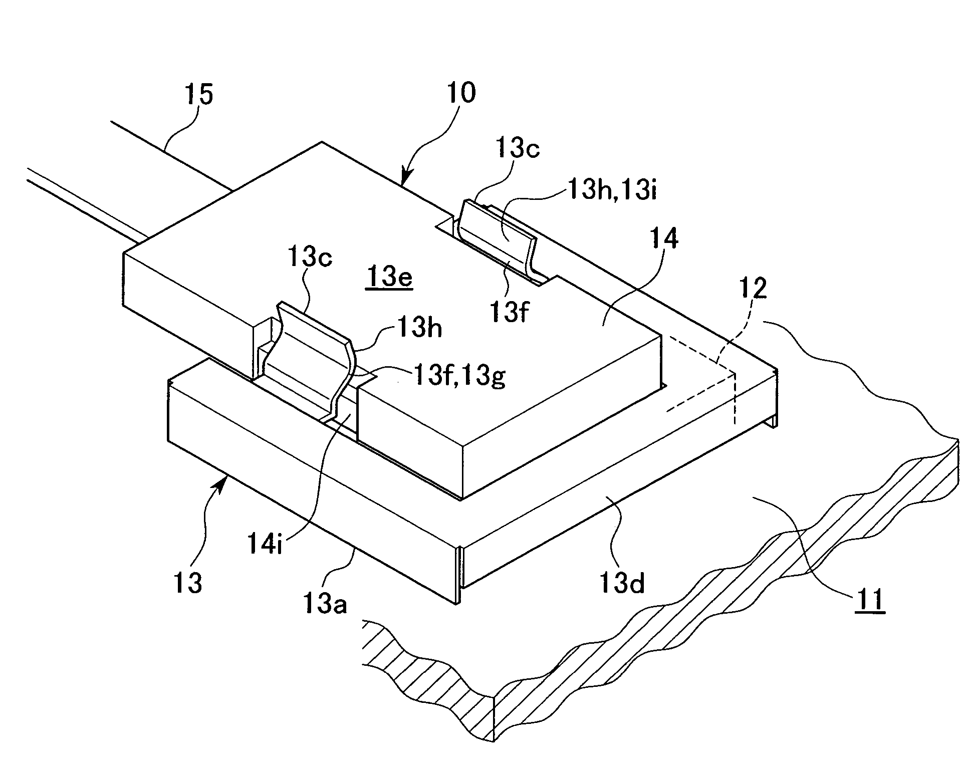
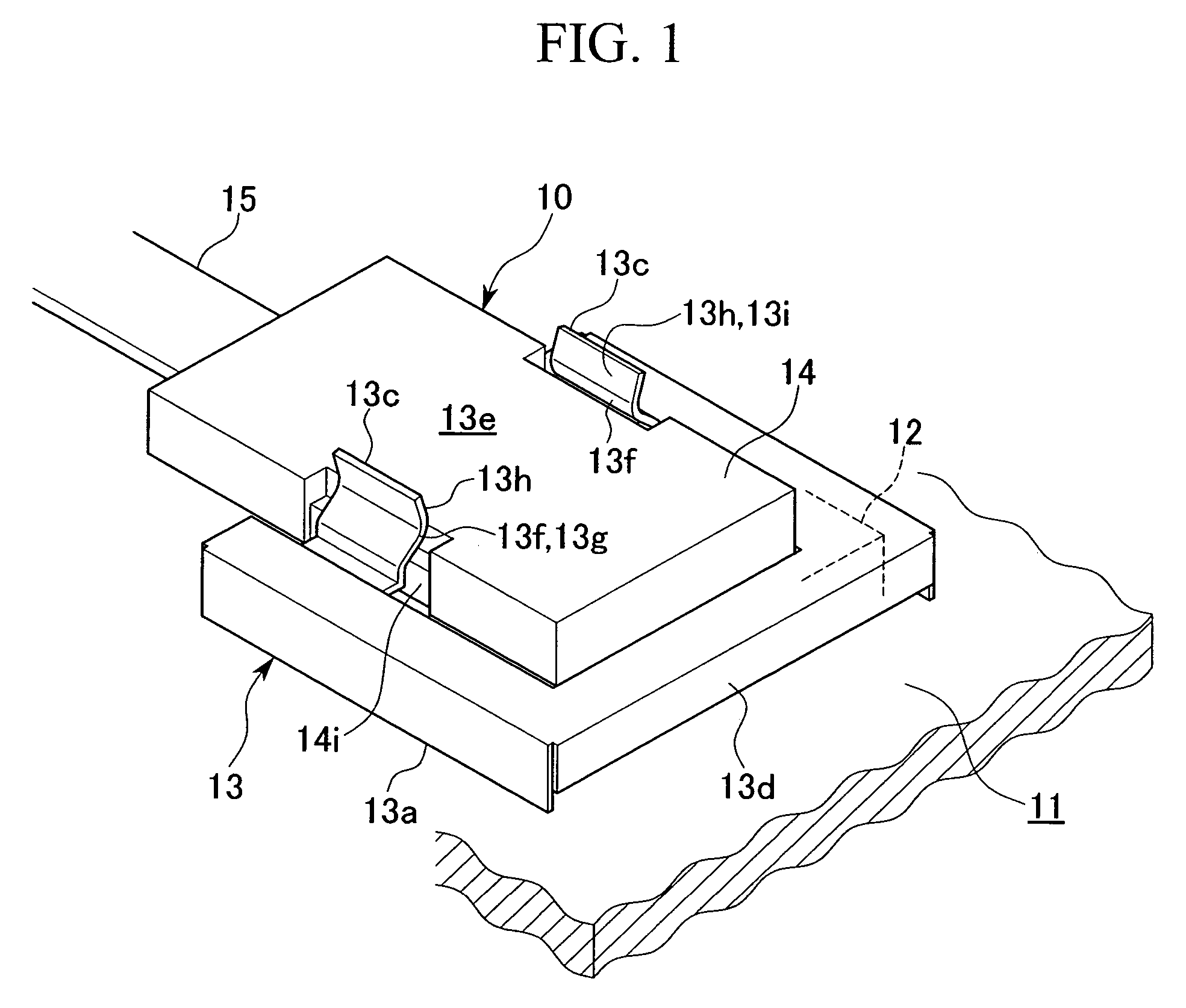
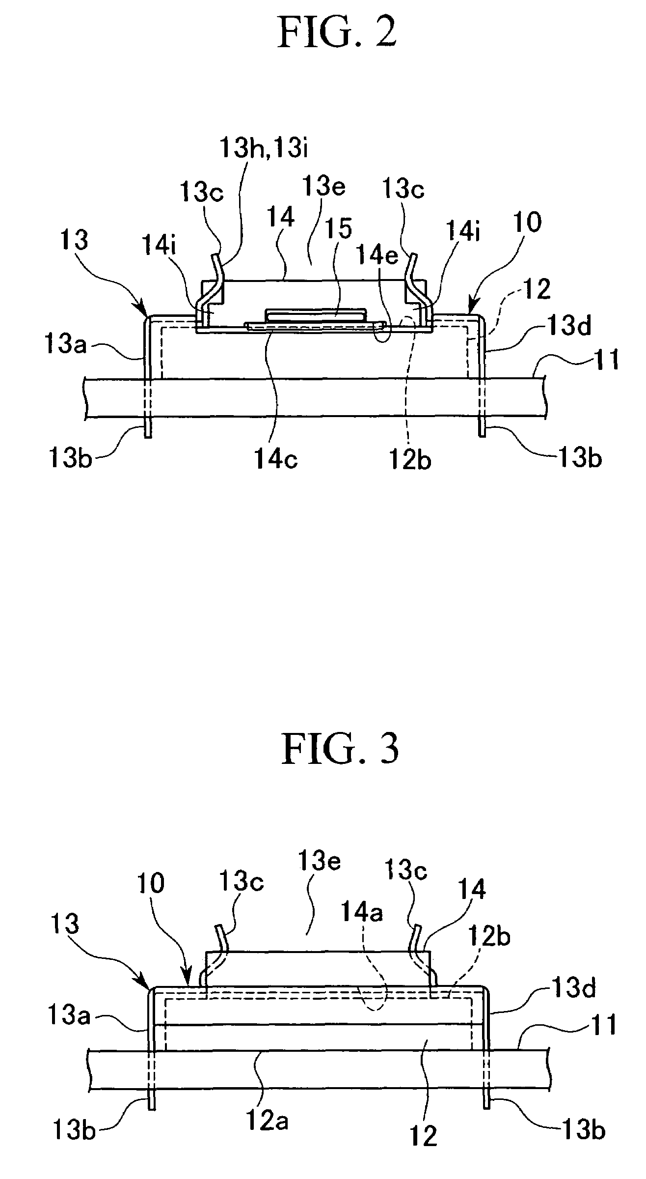
[0041]FIG. 1 is an overall perspective view showing the structure of an optical transceiver 10 (an optical transceiver of the type which is installed upon a substrate) according to the present invention, while FIG. 2 is a side view thereof (the side where a coated optical fiber 15 comes out), FIG. 3 is a side view of the optical transceiver of FIG. 1 from the opposite side to that of FIG. 2, and FIG. 4 is an elevational sectional view thereof.

[0042]In FIGS. 1 through 4, the reference numeral 11 denotes a circuit board (a substrate), while 12 denotes a photoelectric conversion module, 13 denotes a connector holder, 14 denotes an optical connector, and 15 denotes a coated optical fiber (core wire). Although the coated optical fiber of this embodiment is one in which a plurality of optical fibers 15a which are sheathed with plastic or the like are juxtaposed and bundled, the present invention is not limited to this.

[0043]The photoelectric conversion module 12 of this embodiment is a ch...

embodiment 2

[0082]FIG. 7 is a perspective view showing a connector main body 22 of an optical connector of the second embodiment as seen upside down, FIG. 8 is a plan view thereof, FIG. 9 is an A-A sectional view of FIG. 8, FIG. 10 is a B-B sectional view of FIG. 9, FIG. 11 is a C-C sectional view of FIG. 9, FIG. 12 is a view of a state in which a coated optical fiber ribbon has been inserted into the connector main body 22 of FIG. 8, FIG. 13 is a sectional view showing a situation in which an optical connector 21 which has been made using the above described connector main body 22 is being used, and FIG. 14 is an enlarged view of an essential portion of FIG. 13.

[0083]The optical connector 21 of this embodiment, as shown in FIGS. 13 and 14, is one for optically connecting together an optical fiber 32 which constitutes an optical path, and an optical device 25 of an optical transceiver 24 which transmits and receives optical signals. The optical transceiver 24 is mounted on a circuit board 26 wi...


PUM


Abstract

An optical transceiver 10 includes an optical device 16 which is provided upon a substrate 11, an optical connector 14 which is connected to an optical fiber 15a, and a connector holder 13 for optically connecting together the optical device and the optical connector 14. The connector holder 13 includes an engagement means 13c which holds the optical connector 14. The engagement means 13c holds the optical connector 14 when the optical connector 14 is pressed in towards the substrate. The optical connector 14 supports the optical fiber 15a so that the optical axis of the optical fiber 15a subtends a fixed angle with respect to the optical axis of the optical device 16. And the optical connector 14 includes a mirror 14g for optically connecting between the optical device 16 and the optical fiber 15a.

Description

TECHNICAL FIELD[0001]The present invention relates to an optical transceiver for installing an optical connector which is provided at the tip end of an optical fiber to a circuit board upon which is installed an optical device (optical element), which may be a light emitting device and / or a light receiving device, while determining its position at a position at which said optical device and said optical fiber can be optically connected together; and to an optical connector which is fitted upon a tip end portion of an optical fiber, which is disposed so as to be face to face with an optical input and output terminator which is directly or indirectly installed upon a circuit board, and which optically connects between the optical fiber and the optical input and output terminator.[0002]Priority is claimed on Japanese Patent Applications Nos. 2003-125378 and 2003-125915 (both filed on Apr. 30, 2003), the contents of which are incorporated herein by reference.BACKGROUND ART[0003]Nowadays...

Claims


Application Information

Patent Timeline
Patent Type & Authority Patents(United States)
IPC IPC(8): G02B6/36G02B6/30G02B6/42
CPCG02B6/4214G02B6/4249G02B6/4292
Inventor FUJIWARA, KUNIHIKONISHIMURA, AKITOHAYASHI, YUKIONOZAWA, TETSUOSHIMIZU, TAKANORIHATAKEYAMA, ICHIROKURATA, KAZUHIKO
Owner NEC CORP
Why Eureka
Try Eureka