
Liquid crystal display device, and method of driving the same

Inactive Publication Date: 2009-05-19
SEMICON ENERGY LAB CO LTD
View PDF49 Cites 18 Cited by
  • Summary
  • Abstract
  • Description
  • Claims
  • Application Information

AI Technical Summary

Benefits of technology

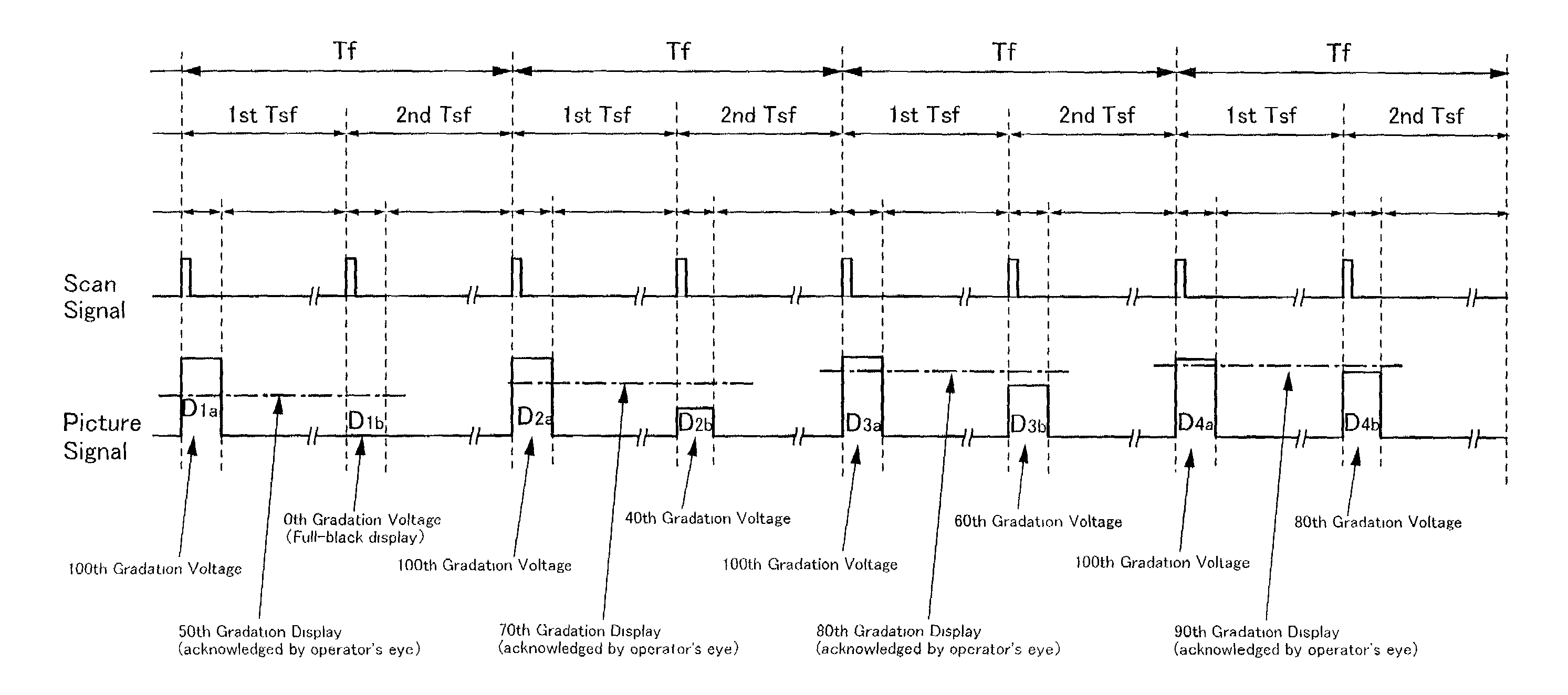
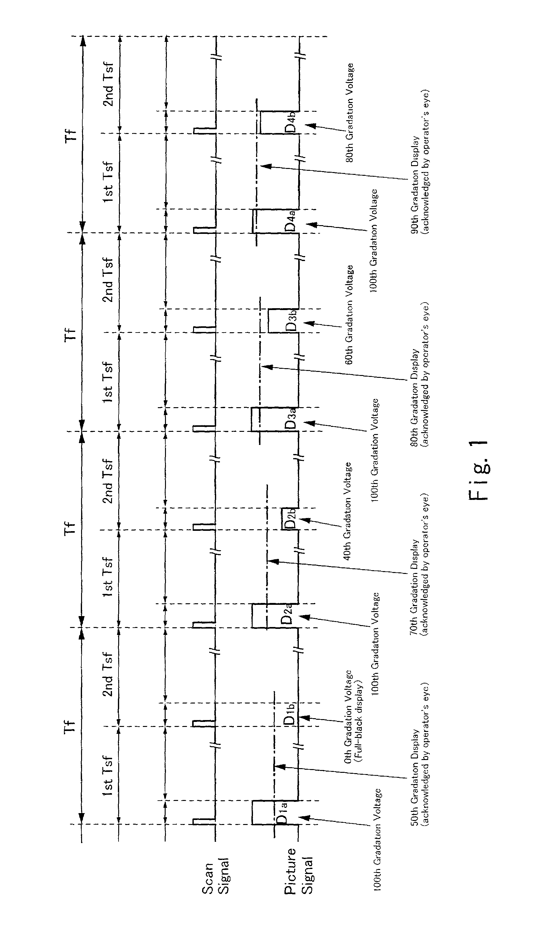
[0019]In light of the above-mentioned problems, an object of the present invention is to provide a liquid crystal display device making it possible to reduce flicker and afterimages and display highly minute pictures.

Problems solved by technology

Therefore, the time for writing picture signals in the pixels is long so that flicker is generated to be conspicuous.
When gradation display is performed, there arises a problem that afterimages are liable to stand out because of a long response time of liquid crystal.
Particularly in the case that moving images are displayed. afterimages cause a big problem.

Method used


Image

  • Liquid crystal display device, and method of driving the same
  • Liquid crystal display device, and method of driving the same
  • Liquid crystal display device, and method of driving the same

Examples


example 1

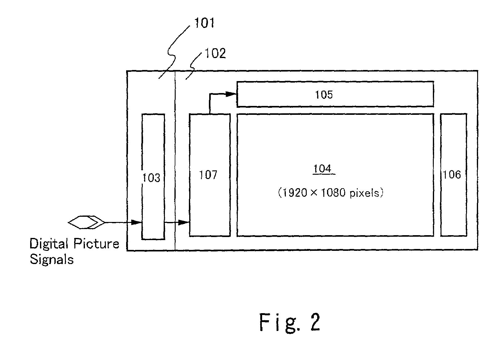
[0072]FIG. 2 schematically illustrates a configuration of the liquid crystal display device of the present invention. This liquid crystal display device has, on an active matrix substrate 101, a source driver 105, a gate driver 106, a digital video data dividing circuit 107, a pixel portion 104 in which plural pixel TFTs are arranged in a matrix form, and a flexible print circuit (FPC) terminal 103. In the liquid crystal display device, this active matrix substrate 101 and a counter substrate 102 are attached to each other with an adhesive agent such as a sealant, and a liquid crystal is held therebetween. The source driver 105 and the gate driver 106 drive the pixel TFTs in the pixel portion. The counter substrate 102 has a counter electrode (not illustrated). Various signals are inputted from the outside to the FPC terminal 103.

[0073]FIG. 3 illustrates the configuration of the source driver of the liquid crystal display device of the present example in more detail, in which the sa...

example 2

[0095]In the present example, a structural example of the liquid crystal module to which the driving method of the present invention is applied will be described, referring to FIGS. 5-7.

[0096]FIG. 5 illustrates a top view of a pixel portion in the present example, wherein illustration of the side of a counter substrate is omitted. A portion surrounded by a dot line frame 200 represents one pixel portional views of portions shown by dot lines α-α′ and β-β′ in FIG. 6A are illustrated by dot lines α-α′ and β-β′ in FIG. 6B. Each pixel has a semiconductor layer 201, a lower light-shielding film 202, a source signal line 203, a gate electrode 204 and a connecting electrode 205, a retaining capacitor 206 and a pixel electrode 207. The retaining capacitor of the pixel is formed between a semiconductor layer connected electrically to the semiconductor layer of the pixel TFT and an interconnection formed in the same layer as the gate electrode.

[0097]When the pixel portion is formed, it is des...

example 3

[0102]In the present example, an example wherein the liquid crystal module of Example 2 is applied to a view finder for a video camera will be described.

[0103]In FIG. 8, reference number 1001 represents a video camera body; reference number 1002, a liquid crystal panel; reference number 1003, a view finder; reference numbers 1004 and 1005, operation switches; and reference number 1006, a lens. In the video camera illustrated in FIG. 8, pictures taken in from the lens 1006 are converted to picture signals by CCD imaging elements, and then the picture signals are recorded on a recording medium. The liquid crystal panel 1002 and the view finder 1003 are display devices for displaying the picture signals.

[0104]While an operator observes pictures displayed on the view finder 1003, the operator can take images of an object. The view finder 1003 has a small-sized liquid crystal module, and the operator can observe pictures displayed on this small-sized liquid crystal module.

[0105]Since pic...


PUM


Abstract

In driving a liquid crystal display device, respective voltages of picture signals supplied in subframe periods are changed so as to enlarge a voltage difference between a gradation voltage of a picture signal supplied in the first subframe period and a gradation voltage of a picture signal supplied in the second subframe period.

Description

BACKGROUND OF THE INVENTION[0001]1. Field of the Invention[0002]The present invention relates to a liquid crystal display device having a circuit composed of a thin film transistor, which may be referred to as a TFT hereinafter, and a method of driving the same. The present invention relates to, for example, an electro-optical device, a typical example of which is a liquid crystal display panel, and an electronic instrument on which such an electro-optical device is mounted as a component.[0003]2. Description of Related Art[0004]In recent years, attention has been paid to the technique of using a semiconductor thin film (thickness: about several nanometers to several hundreds of nanometers) formed on a substrate having an insulated surface to make thin film transistors (TFTs). A thin film transistor is widely applied to electronic devices such as an IC and an electro-optical device. It is particularly desired to develop the thin film transistor as a switch element of a liquid crysta...

Claims


Application Information

Patent Timeline
IPC IPC(8): G09G3/36G09G5/10G02F1/133G09G3/20
CPCG09G3/2011G09G3/3648G09G3/2025G09G2320/0247
Inventor HIROKI, MASAAKI
Owner SEMICON ENERGY LAB CO LTD
Learn More