Voltage controlled oscillator circuit with different sized shunt transistors
a voltage control and transistor technology, applied in the direction of pulse generator, pulse manipulation, pulse technique, etc., can solve the problems of phase noise increase, phase noise deterioration, and current in the voltage to current converter circuit is also decreased, so as to prevent deterioration of phase noise characteristics and expand the frequency range
- Summary
- Abstract
- Description
- Claims
- Application Information
AI Technical Summary
Benefits of technology
Problems solved by technology
Method used
Image
Examples
first embodiment
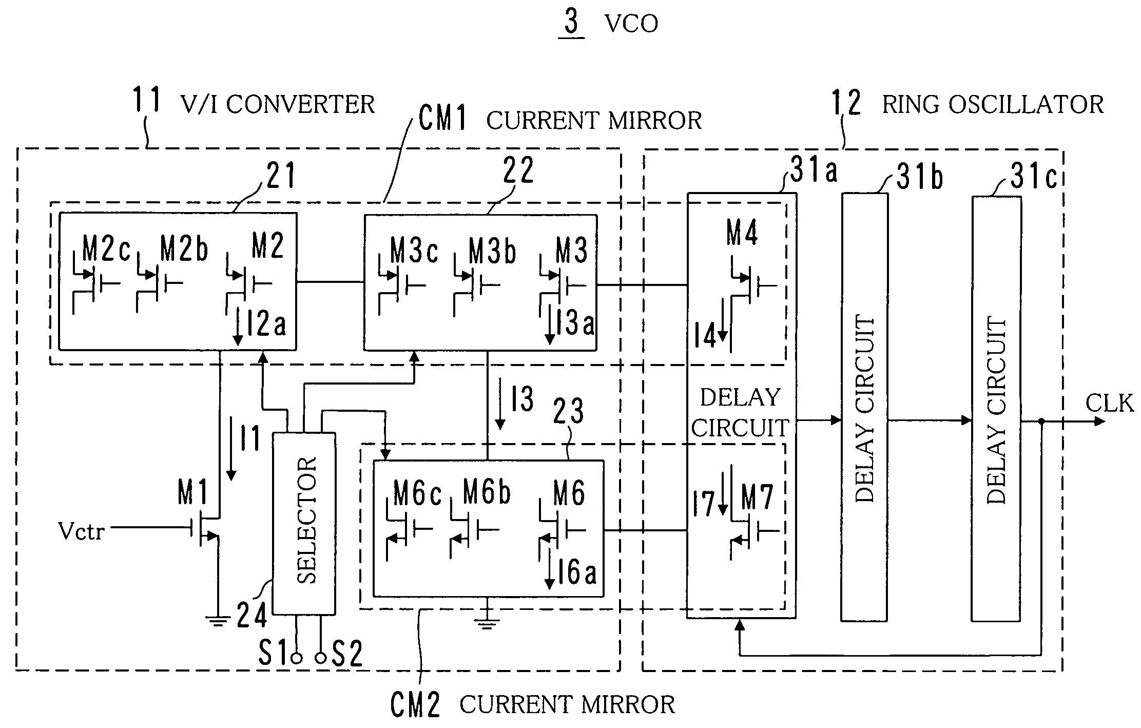
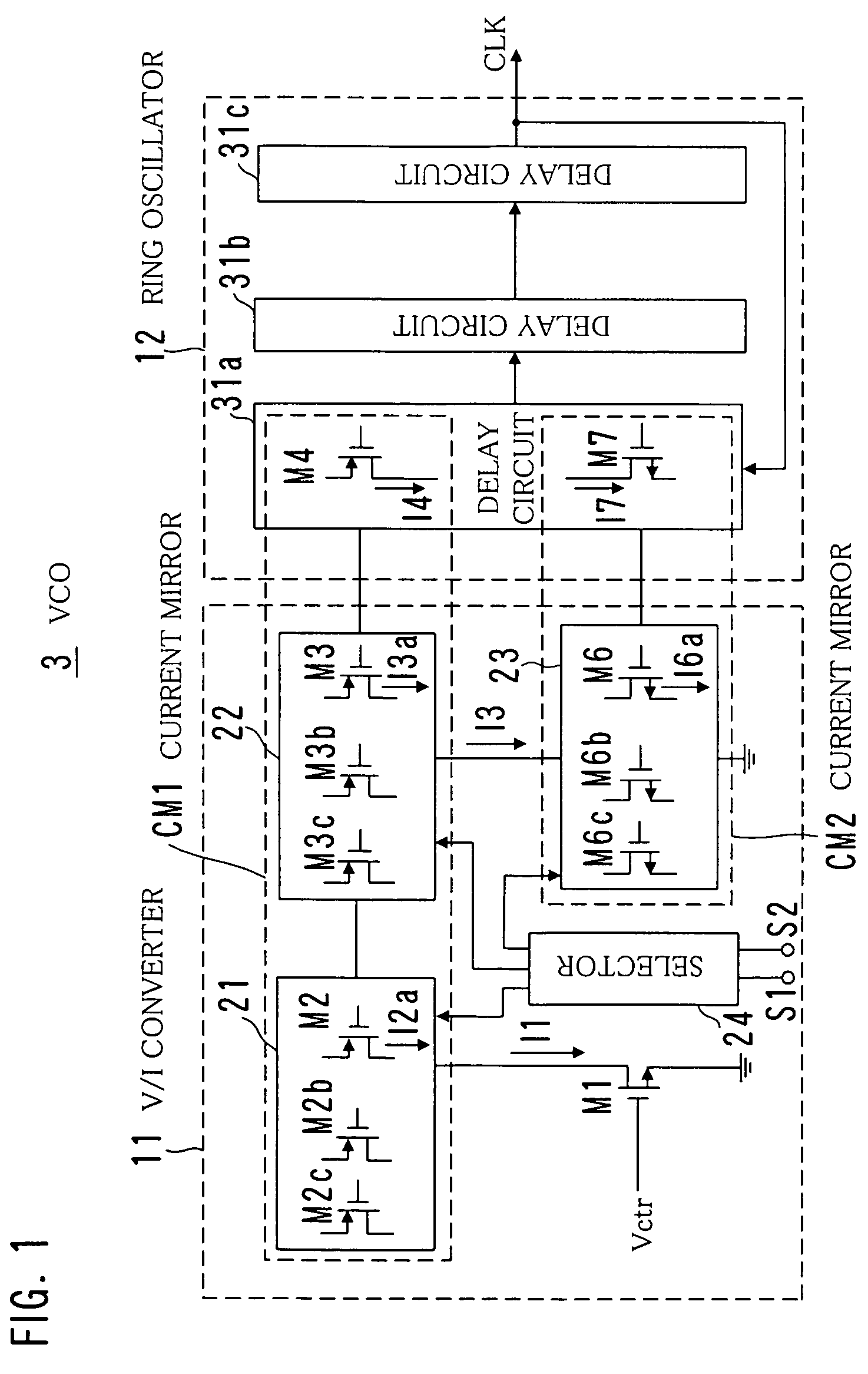
[0046]FIG. 1 is a circuit diagram of a VCO 3 according to a first embodiment of the present invention.
[0047]As shown in FIG. 1, the VCO 3 is made up of a voltage to current converter circuit 11 and a ring oscillator 12.
[0048]The voltage to current converter circuit 11 converts input voltage (control voltage) Vctr that is supplied to the VCO 3 into current I1, and current that flows in the ring oscillator 12 is controlled in accordance with the generated current I1 so that an oscillation frequency is altered.
[0049]The ring oscillator 12 is made up of a plurality of delay circuits 31a, 31b and 31c that are connected like a ring. Although three delay circuits 31 are used in this embodiment, it is possible to use five, seven or other number of delay circuits. An oscillation frequency of the ring oscillator 12 alters in accordance with current flowing in each delay circuit 31. For example, as the current increases, the oscillation frequency is raised because a capacitance existing in the...
second embodiment
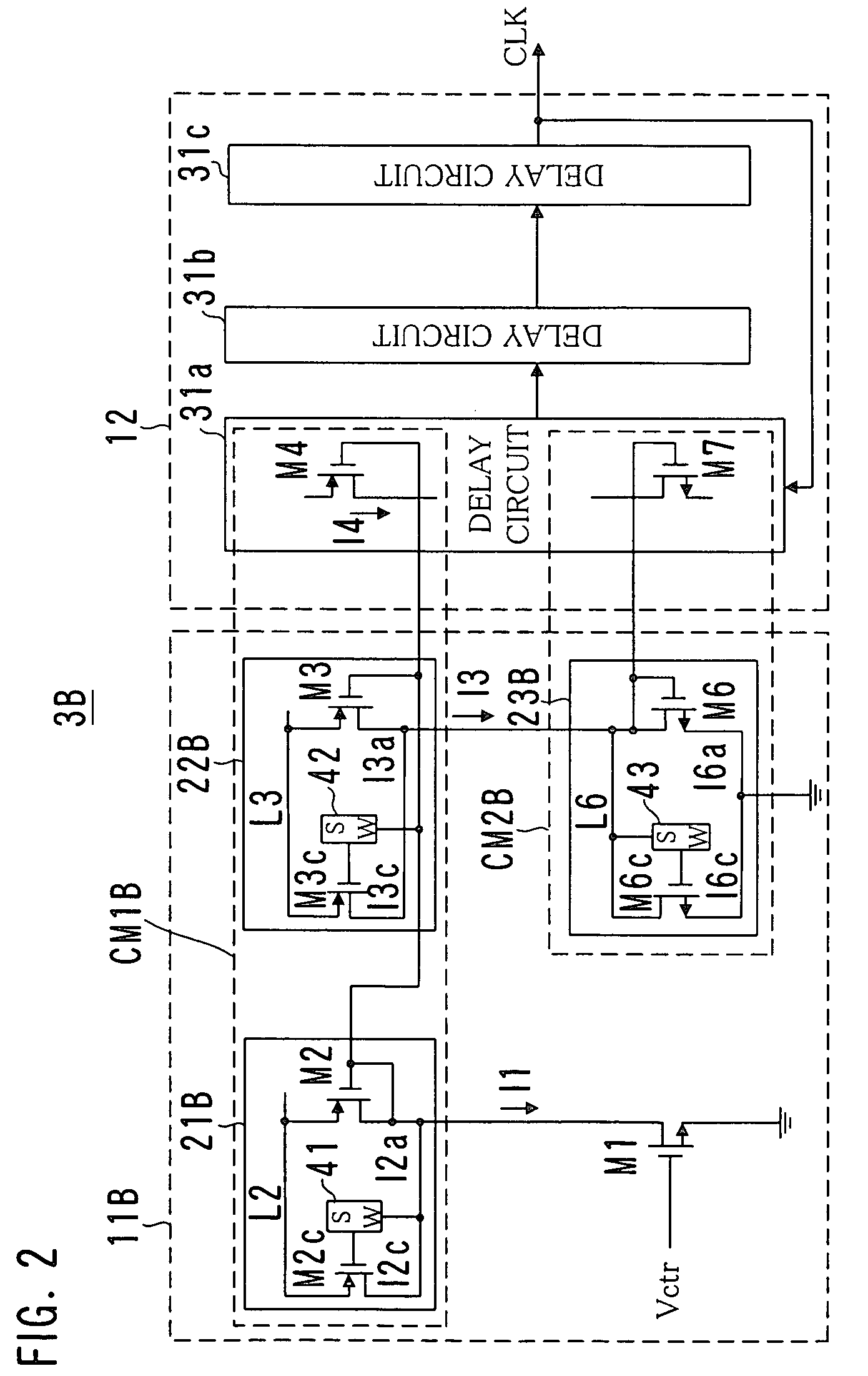
[0079]FIG. 2 is a circuit diagram of a VCO 3B according to a second embodiment of the present invention.
[0080]The VCO 3B shown in FIG. 2 is provided with switching circuits 41-43 for turning on and off the transistors M2b, M2c, M3b, M3c, M6b and M6c that can be connected in parallel, and they are disposed between gates and drains of the transistors, respectively. Note that lines L2 and L3 are power source lines.
[0081]In FIG. 2, circuits for the transistors M2b, M3b and M6b and the selector 24 are omitted. It is the same in the following drawings.
[0082]When the switching circuits 41-43 are selectively turned on or off by the selector 24, the gate and the drain are selectively connected to each other or separated from each other, respectively. Thus, any one of the transistors M2b, M2c, M3b, M3c, M6b and M6c is connected in parallel with the transistors M2, M3 and M6, respectively.
third embodiment
[0083]FIG. 3 is a circuit diagram of a VCO 3C according to a third embodiment of the present invention.
[0084]The VCO 3C shown in FIG. 3 is provided with switching circuits 44-46 for turning on and off the transistors M2b, M2c, M3b, M3c, M6b and M6c that can be connected in parallel, and they are disposed between sources of the transistors and the lines L3, L4 and L6, respectively.
[0085]When the switching circuits 44-46 are selectively turned on or off by the selector 24, the gates and lines L3, L4 and L6 are selectively connected to each other or separated from each other, respectively. Thus, any one of the transistors M2b, M2c, M3b, M3c, M6b and M6c is connected in parallel with the transistors M2, M3 and M6, respectively.
PUM
 Abstract
Description
Claims
Application Information


