Sealing structure of field emission display device and method of manufacturing the same

a field emission display and sealing structure technology, applied in the manufacture of electric discharge tubes/lamps, vacuum obtaining/maintenance, discharge tubes luminescnet screens, etc., can solve the problems of serious deterioration of carbon nano-tube emission characteristics, easy oxidation of carbon nano-tubes in high temperature processes, etc., to reliably seal the inside of the fed device, reduce the height of frit, easy to exhaust

Inactive Publication Date: 2009-06-02
SAMSUNG SDI CO LTD
View PDF13 Cites 0 Cited by
  • Summary
  • Abstract
  • Description
  • Claims
  • Application Information

AI Technical Summary

Benefits of technology

[0009]The present invention provides a sealing structure of a field emission display (FED) device for preventing the deterioration of an emission characteristic of carbon nanotubes, and reducing a process time and a number of steps in a high temperature process by improving the shape and manufacturing method of a frit which seals the FED device, and a method of manufacturing the same.
[0018]According to still another aspect of the present invention, there is provided a method of manufacturing a sealing structure of an FED device by arranging a lower substrate and an upper substrate, forming spacers between the lower substrate and the upper substrate, forming a frit, which is longer than the spacer by a predetermined length, separated from the spacer by a predetermined distance, and heating the lower substrate and the upper substrate while arranging the upper substrate on the lower substrate to reduce the height of the frit in order for the spacers to contact the lower substrate and the upper substrate.
[0019]The frit may include at least one exhaust hole. According to the sealing structure of the FED device, the inner gas can be easily exhausted because the frit includes exhaust grooves or exhaust holes.
[0020]In addition, the sealing structure of the FED device manufactured according to the principles of the present invention can reliably seal the inside of the FED device while preventing the damage of the spacers.

Problems solved by technology

In such a packaging process described above, however, carbon nano-tubes are easily oxidized in high temperature process due to the oxygen remaining in the firing furnace.
In fact, during the packaging process, a large number of the carbon nano-tubes are oxidized, and the emission characteristic of carbon nano-tubes seriously deteriorates.

Method used


Image

  • Sealing structure of field emission display device and method of manufacturing the same
  • Sealing structure of field emission display device and method of manufacturing the same
  • Sealing structure of field emission display device and method of manufacturing the same

Examples


first embodiment

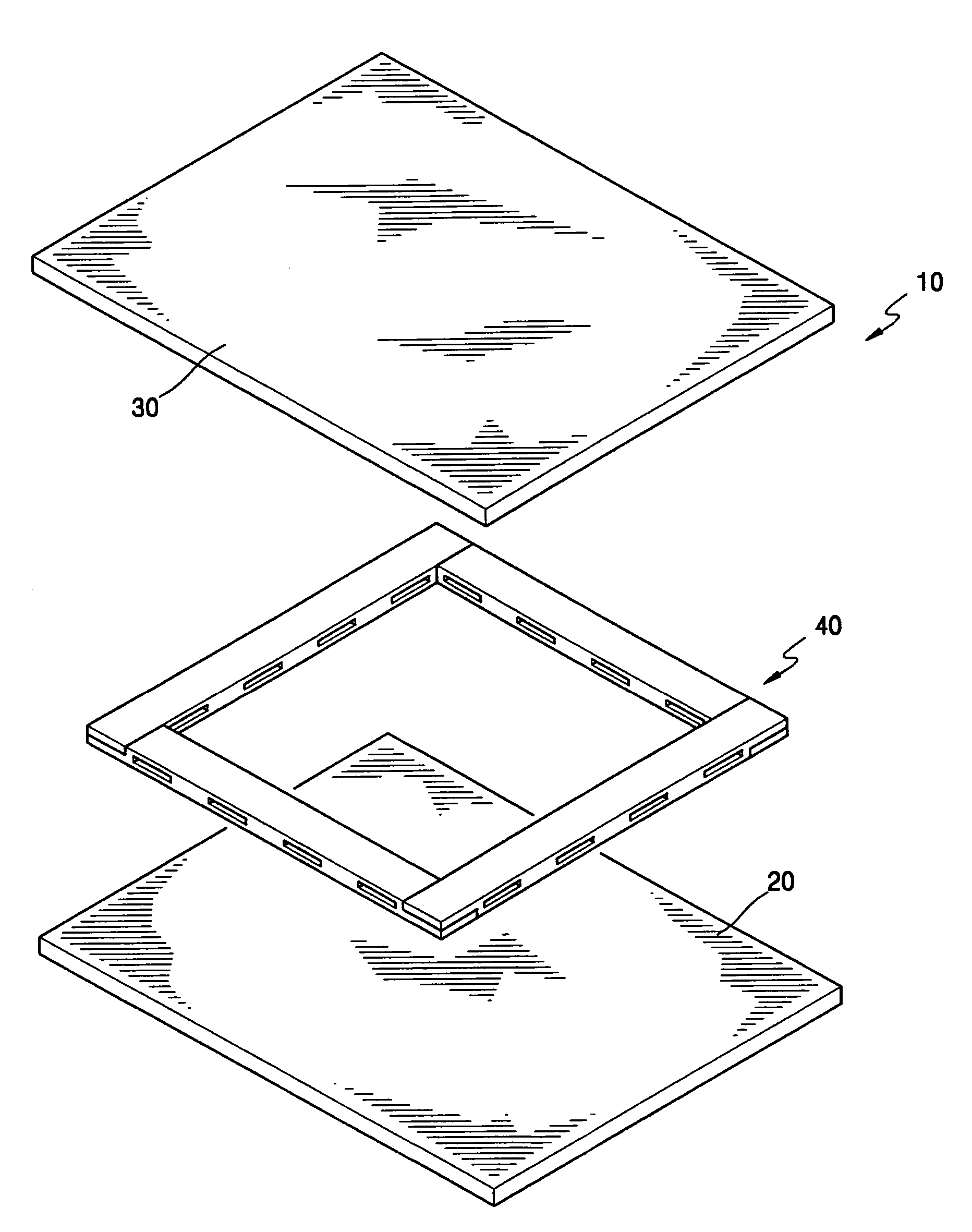
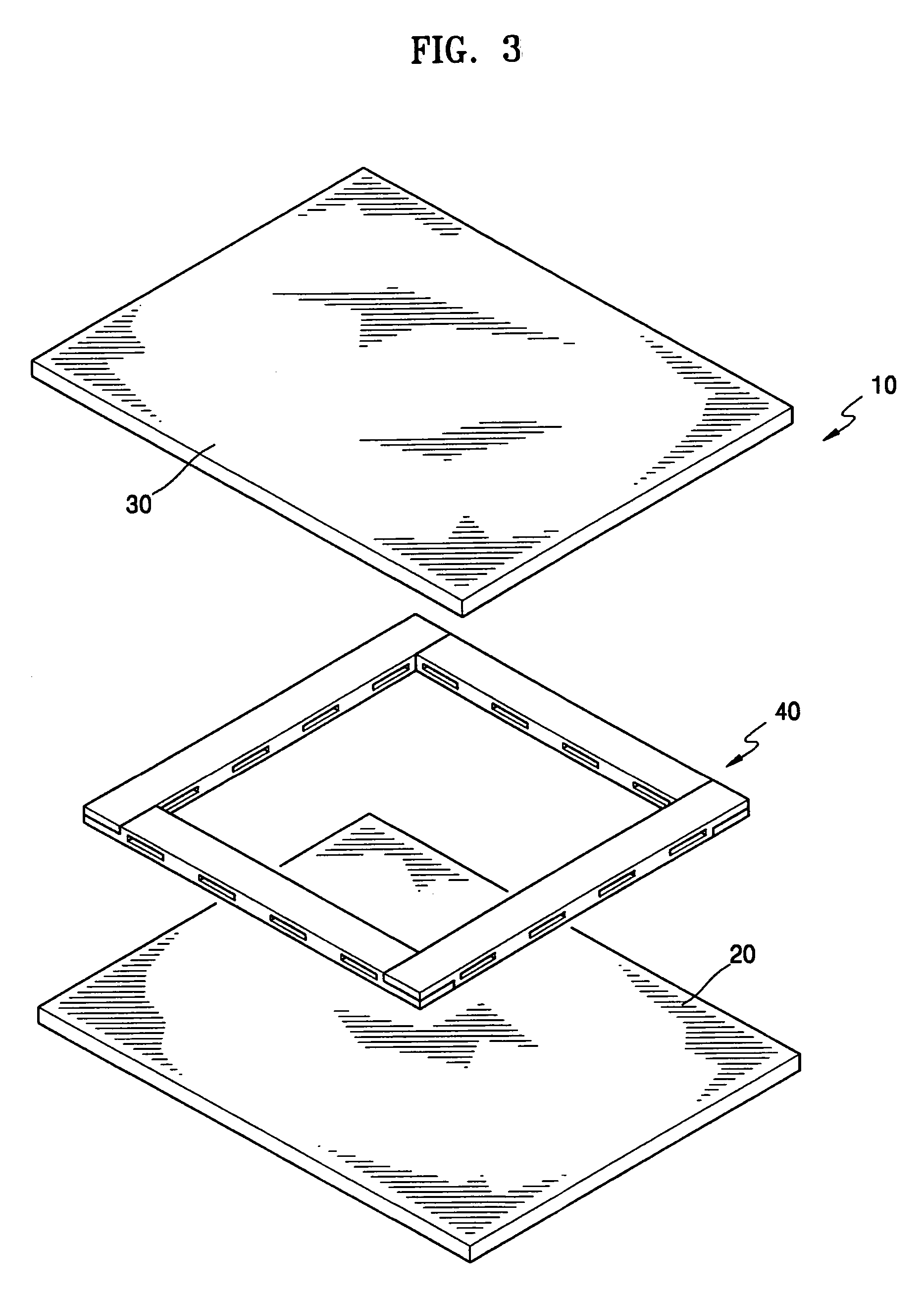
[0043]FIG. 4 is a perspective view of a frit for a sealing structure of a FED device according to the present invention. Referring to FIG. 4, the frit 40A includes a base 41, convex units 42 formed on the base 41 with predetermined intervals, and concave units 43 formed between the convex units 42. In this case, the concave units 43 operate as exhaust grooves to exhaust inner gas from the FED device. Multiple concave units 43 may be formed with predetermined intervals in order to increase an amount of exhaust through the frit 40A.

[0044]When an inert gas such as nitrogen is injected into the FED device in a firing furnace as a substitute for the inner gas in the FED device, the exhausting speed and the amount of inner gas exhausted from the FED device are improved, because the frit 40A includes the convex units 42 and the concave units 43. Therefore, the inner gas in the FED device can be easily exhausted from the FED device.

second embodiment

[0045]FIG. 5 is a perspective view of a frit for a sealing structure of a FED device according to the present invention. Referring to FIG. 5, the frit 40B includes a base 41, convex units 42 and concave units 43 formed on the base 41, and connection units 44 formed at both ends of the base 41. Since the frit 40B includes the connection units 44, the frit 40B can be easily connected with another frit 40B.

[0046]FIG. 6 is a perspective view illustrating an example of a combination of the frits 40B from FIG. 5 to complete a frit 40. Referring to FIG. 6, the frits 40B are combined by having a connection unit 44 of a frit 40B engage with connection unit 44 of another frit 40B. In this case, the frits 40B can be combined while forming a predetermined angle therebetween, for example, a right angle.

[0047]The angle between the frits 40B can be easily controlled. Accordingly, the combination angle of the frits 40B can be controlled based on the sealing structure of the FED device. Therefore, a...

third embodiment

[0050]FIG. 8 is a perspective view of a frit for a sealing structure of an FED device according to the present invention. Referring to FIG. 8, the frit 40C includes a body unit 45 and exhaust holes 46 formed in the body unit 45. A plurality of exhaust holes 46 may be formed while having predetermined intervals in order to increase an amount of exhaust through the frit 40C.

[0051]Since the exhaust holes 46 are formed in the body unit 45 of the frit 40C, the frit 40C can exhaust inner gas of the FED device, even without directly contacting another member, for example, an upper substrate 30 or a lower substrate 20. Accordingly, the arrangement of the frit 40C is not limited, and can be optimally selected to realize a required sealing structure of the FED device.


PUM


Abstract

A sealing structure for a field emission display (FED) device and a method of manufacturing the same is provided. The sealing structure includes an upper substrate, a lower substrate, spacers, and a frit, wherein at least one exhaust outlet is formed in the frit. The method of manufacturing the sealing structure of the FED device prepares a lower substrate and an upper substrate, installs a frit having at least one exhaust outlet between the lower substrate and the upper substrate, and heats the lower substrate and the upper substrate while arranging the upper substrate on the lower substrate at a predetermined temperature to melt the frit in order to seal the space between the lower substrate and the upper substrate. Inner gas can be easily exhausted and the inside of the FED is reliably sealed while preventing damages of the spacers.

Description

CLAIM OF PRIORITY[0001]This application makes reference to, incorporates the same herein, and claims all benefits accruing under 35 U.S.C. § 119 from an application for SEALING STRUCTURE OF A FILED EMISSION DISPLAY DEVICE, AND A MANUFACTURING METHOD OF THE SAME, earlier filed in the Korean Intellectual Property Office on the 23rd of February, 2005 and there duly assigned Serial No. 10-2005-0015053.BACKGROUND OF THE INVENTION[0002]1. Field of the Invention[0003]The present invention relates to a field emission display (i.e., “FED”) device, and more particularly, to a sealing structure of a FED device and a method of manufacturing the same.[0004]2. Description of the Related Art[0005]In general, a field emission display (i.e., a “FED”) device is one of flat panel display devices, and formed of a tip-shaped or wedge-shaped cathode and an anode on which a fluorescent substance is coated. When electrons emitted from a predetermined portion of the cathode collide with the fluorescent subs...

Claims


Application Information

Patent Timeline
Patent Type & Authority Patents(United States)
IPC IPC(8): H01J1/62H01J61/24H01J19/70
CPCH01J5/20H01J9/261H01J9/385H01J9/39H01J2329/867H01J2209/385H01J2209/389
Inventor SONG, BYONG-GWONSHIN, MOON-JIN
Owner SAMSUNG SDI CO LTD
Why Eureka
Try Eureka