Dioptric element array substrate, image display device and image display apparatus

a technology of image display device and substrate, applied in the direction of optics, lenses, instruments, etc., can solve the problems of reducing the contrast ratio of display, failure to execute the original display operation of the device, and discharge of charges, and achieve excellent display quality and high light use efficiency

Active Publication Date: 2009-06-02
SHARP KK
View PDF8 Cites 4 Cited by
  • Summary
  • Abstract
  • Description
  • Claims
  • Application Information

AI Technical Summary

Benefits of technology

[0045]In the dioptric element array substrate of the present invention, principal rays of beams incident on the first dioptric element array at angles different from each other and converged with the first dioptric element array are collimated with the second and third dioptric element arrays. Accordingly, by use of the dioptric element array substrate of the present invention, an image display apparatus high in light use efficiency and excellent in display quality (color purity, for example) can be provided.

Problems solved by technology

If intense light is incident on such switching elements, the resistance of the elements in the OFF state will decrease, resulting in discharging of charges obtained during voltage application.
Moreover, no normal drive voltage will be applied to portions of the liquid crystal layer corresponding to the regions in which the switching elements and the interconnections are formed, causing failure in execution of the original display operation of the device.
This will cause occurrence of light leakage in the black display state, for example, arising a problem of reduction in the contrast ratio of display.
Reduction of the sizes of such switching elements and interconnections to less than certain levels is difficult due to the limitations in their electric performances, fabrication technology and the like.
This causes insufficient brightness for a liquid crystal projector that projects a smaller panel on a larger screen by magnification.
It is however very difficult to extremely thin the cover glass plate.
In the production method described above, if the cover glass plate for the two-layered microlens array disclosed in the Literature 2 is extremely thinned, the cover glass plate may possibly be completely ground off due to the variation in the thicknesses of the base glass plates (about ±5 μm), resulting in damage to the second microlens array.
If the thickness of the cover glass plate is set at 5 μm or more to prevent this problem, however, the beams will fail to be converged at positions very near the liquid crystal layer, that is, very near the light outgoing-side surface of the cover glass plate, resulting in low light use efficiency.
However, a variation in etching amounts of about ±5 μm to 10 μm also occurs in this method, and thus the same problem arises.
As described above, when the two-layered microlens array substrate of the Literature 2 is used for a liquid crystal display apparatus, the light use efficiency improves compared with the case of using the single-layered microlens array substrate of the Literature 1, but the display is not yet sufficiently bright.
Moreover, the parallelism of the light outgoing from the microlens array substrate is not sufficiently high, and this results in insufficient color purity, for example.
Also, the above problem occurs, not only in the microlens array substrate, but also in other dioptric element array substrates (microprism array substrate, for example) having dioptric elements arranged two-dimensionally.

Method used


Image

  • Dioptric element array substrate, image display device and image display apparatus
  • Dioptric element array substrate, image display device and image display apparatus
  • Dioptric element array substrate, image display device and image display apparatus

Examples


Embodiment Construction

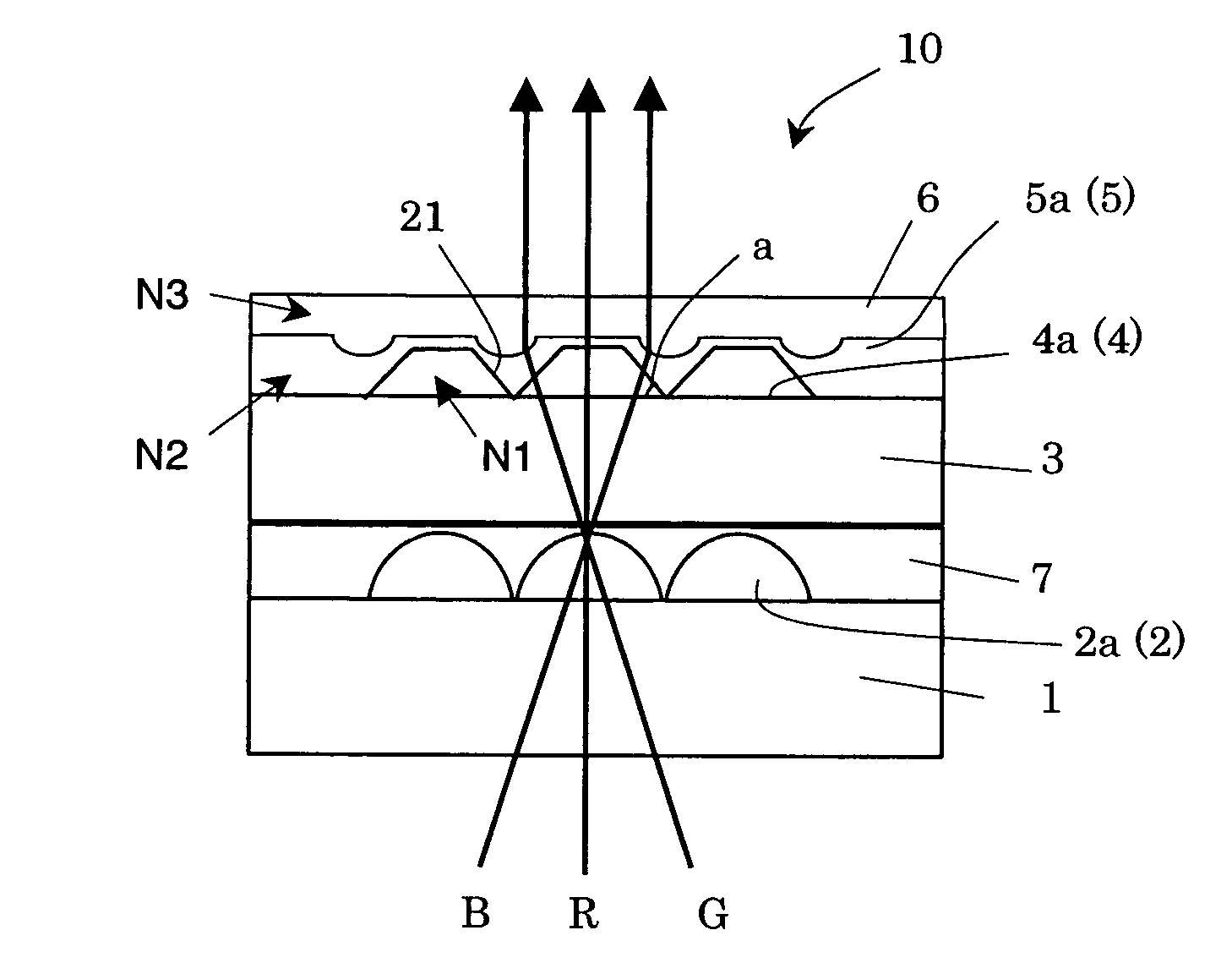
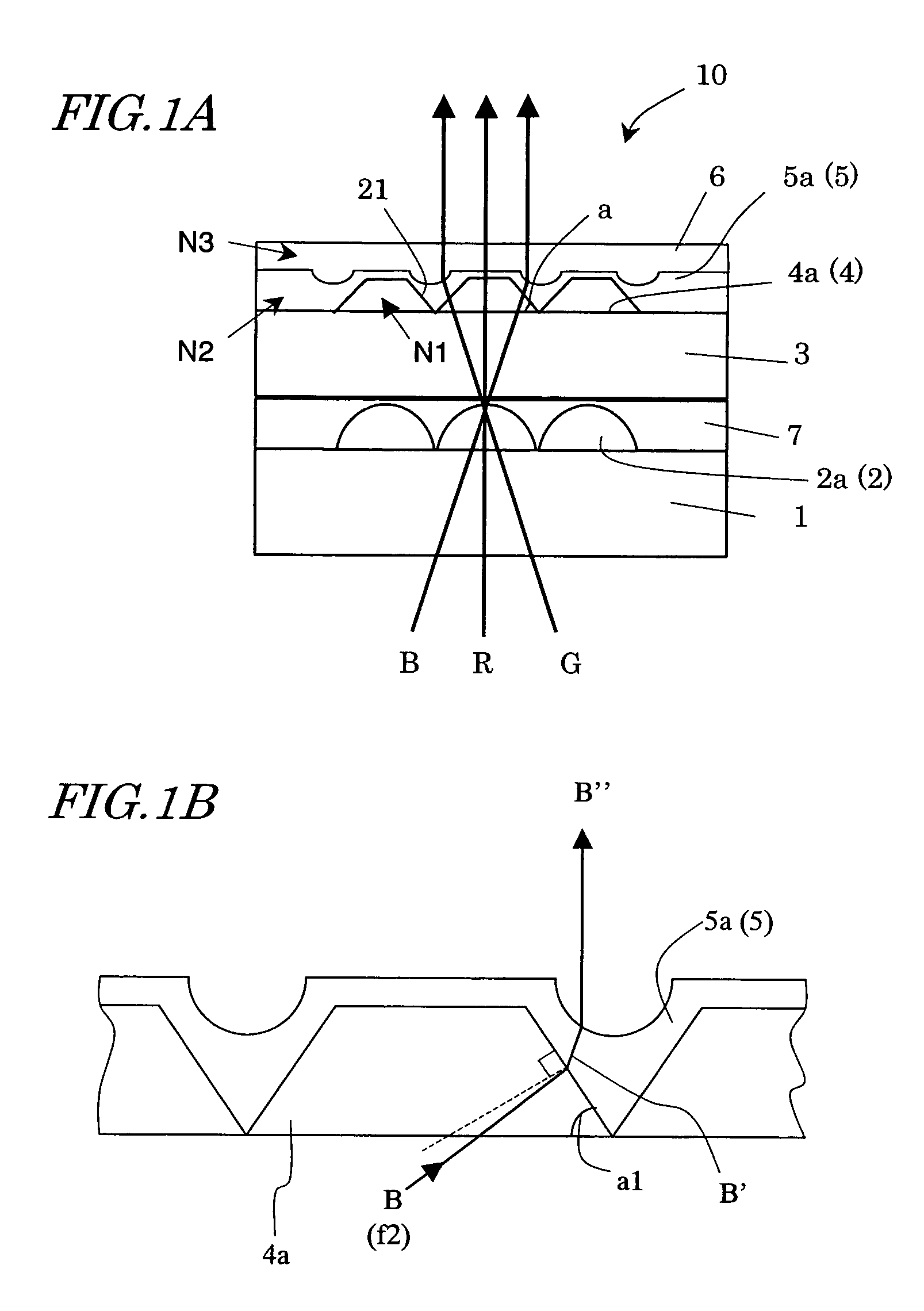
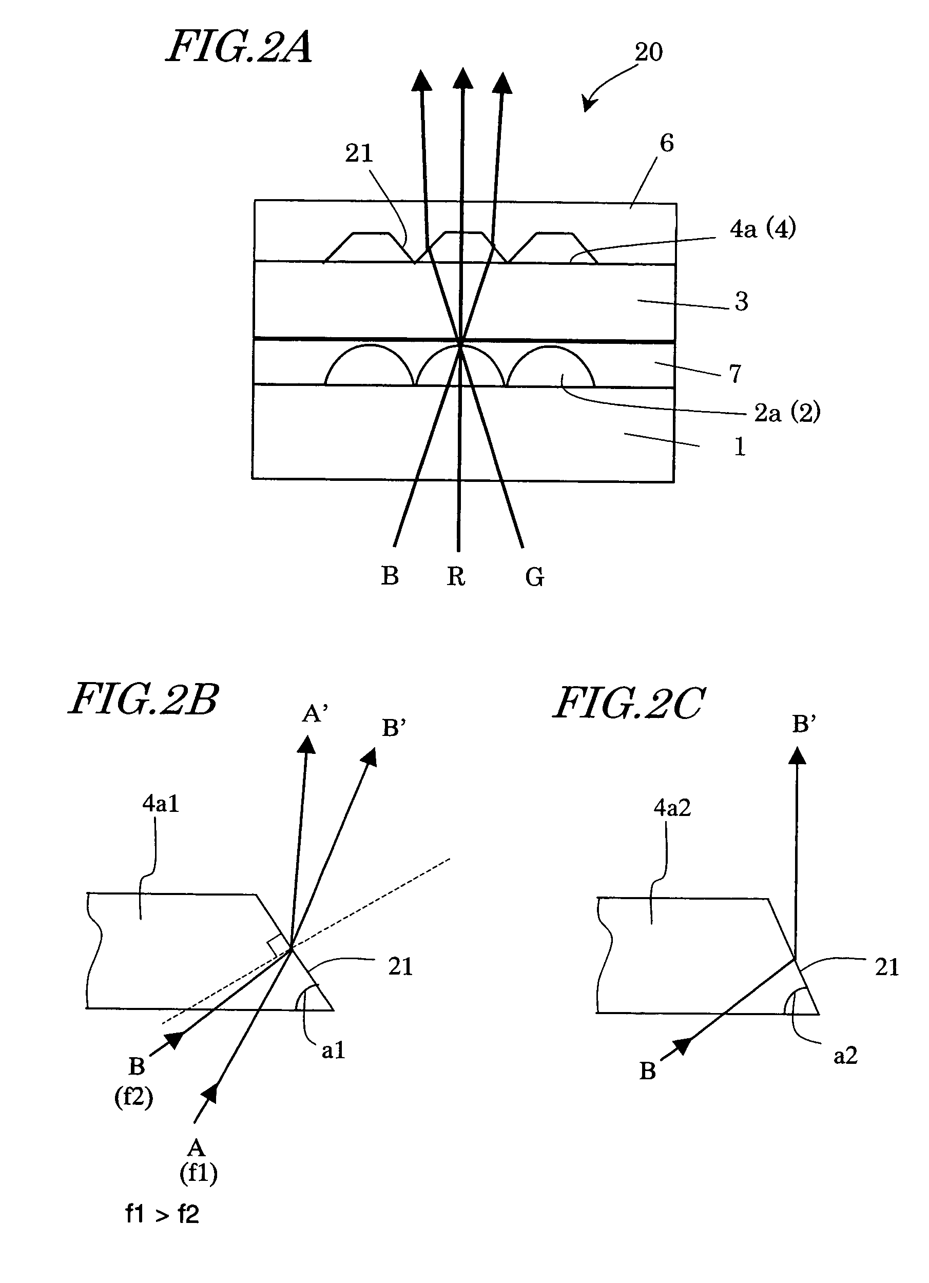
[0058]Hereinafter, the construction and operation of a dioptric element array substrate of an embodiment of the present invention, as well as those of an image display device and an image display apparatus having such a substrate, will be described with reference to the relevant drawings. In the following description, a liquid crystal display device is taken as an example of the image display device, and a projection liquid crystal display apparatus (liquid crystal projector) is taken as an example of the image display apparatus. It should however be noted that the present invention is not limited to these examples.

[0059]First, the construction and function of a dioptric element array substrate of an embodiment of the present invention will be described with reference to FIG. 1A. Although a microlens array substrate 10 having microlenses and microprisms is shown as the dioptric element array substrate in FIG. 1A, microlenses and / or microprisms in any combination may be used as the d...


PUM

PropertyMeasurementUnit
thicknessaaaaaaaaaa
thicknessesaaaaaaaaaa
thicknessaaaaaaaaaa

Abstract

A dioptric element array substrate 10 includes: a first dioptric element array 2 having a plurality of first dioptric elements 2a arranged two-dimensionally; a second dioptric element array 4 having a plurality of second dioptric elements 4a having a first refractive index arranged two-dimensionally in one-to-one correspondence with the first dioptric elements; and a third dioptric element array 5 having a second refractive index different from the first refractive index. Principal rays of beams incident on the first dioptric element array at different angles and converged with the first dioptric element array are collimated with the second and third dioptric element arrays.

Description

BACKGROUND OF THE INVENTION[0001]The present invention relates to a dioptric element array substrate (microlens array substrate, for example) having dioptric elements (lenses and prisms, for example) arranged two-dimensionally, and an image display device and an image display apparatus including such a dioptric element array substrate.[0002]In general, in non-light emitting image display apparatuses, the light transmittance (or reflectance) of each of a plurality of pixels is changed with a drive signal, to modulate the intensity of light entering an image display device (display panel) to thereby realize display of an image and a character. Such image display apparatuses include a direct view mode (direct-view image display apparatus) and a projection mode, such as a projector, in which an image and a character are magnified and projected on a screen with a projection optical system (projection image display apparatus).[0003]As the projector (including both front and back projectio...

Claims


Application Information

Patent Timeline
Patent Type & Authority Patents(United States)
IPC IPC(8): G02F1/1335G02B3/00
CPCG02F1/133526G02F2001/133623G02F1/133623
Inventor KUME, YASUHIROOHNISHI, NORIAKIMIZUSAKI, NAOKO
Owner SHARP KK
Why Eureka
Try Eureka