Board device and liquid crystal display device

a liquid crystal display and board technology, applied in non-linear optics, instruments, optics, etc., can solve the problems of reducing the productivity and display characteristics reducing the production efficiency of the liquid crystal display device, etc., and achieving the enhancement of cross-sectional area, productivity and display performance of the board device.

Inactive Publication Date: 2009-06-02
JAPAN DISPLAY CENTRAL CO LTD
View PDF8 Cites 3 Cited by
  • Summary
  • Abstract
  • Description
  • Claims
  • Application Information

AI Technical Summary

Benefits of technology

[0011]That is, the recessed main body groove portion extending along the longitudinal direction of the seal materials is provided between the height adjusting layers each of which is provided between the first substrate and the second substrate between the plurality of seal materials, and the height adjusting layers are provided with the spacer for holding the interval between the first substrate and the second substrate on one principal surface thereof. As a result, the cross-sectional area between the plurality of seal materials between the first substrate and the second substrate is increased by the main body groove portion. Accordingly, air can be further readily discharged from the gap between the first substrate and the second substrate surrounded by the seal materials, and also liquid material, etc. can be further readily injected into the gap between the first substrate and the second substrate surrounded by these seal materials, so that the productivity and display performance of the board device can be enhanced.

Problems solved by technology

Therefore, there is a risk that the production efficiency of the liquid crystal devices may be reduced.
Furthermore, the cell gap between the array substrate and the counter substrate may be deviated and uniformity of the cell gap cannot be kept because air is not released from a part of the image display area, so that the productivity and display characteristics of the liquid crystal devices may be lowered.

Method used


Image

  • Board device and liquid crystal display device
  • Board device and liquid crystal display device
  • Board device and liquid crystal display device

Examples


Embodiment Construction

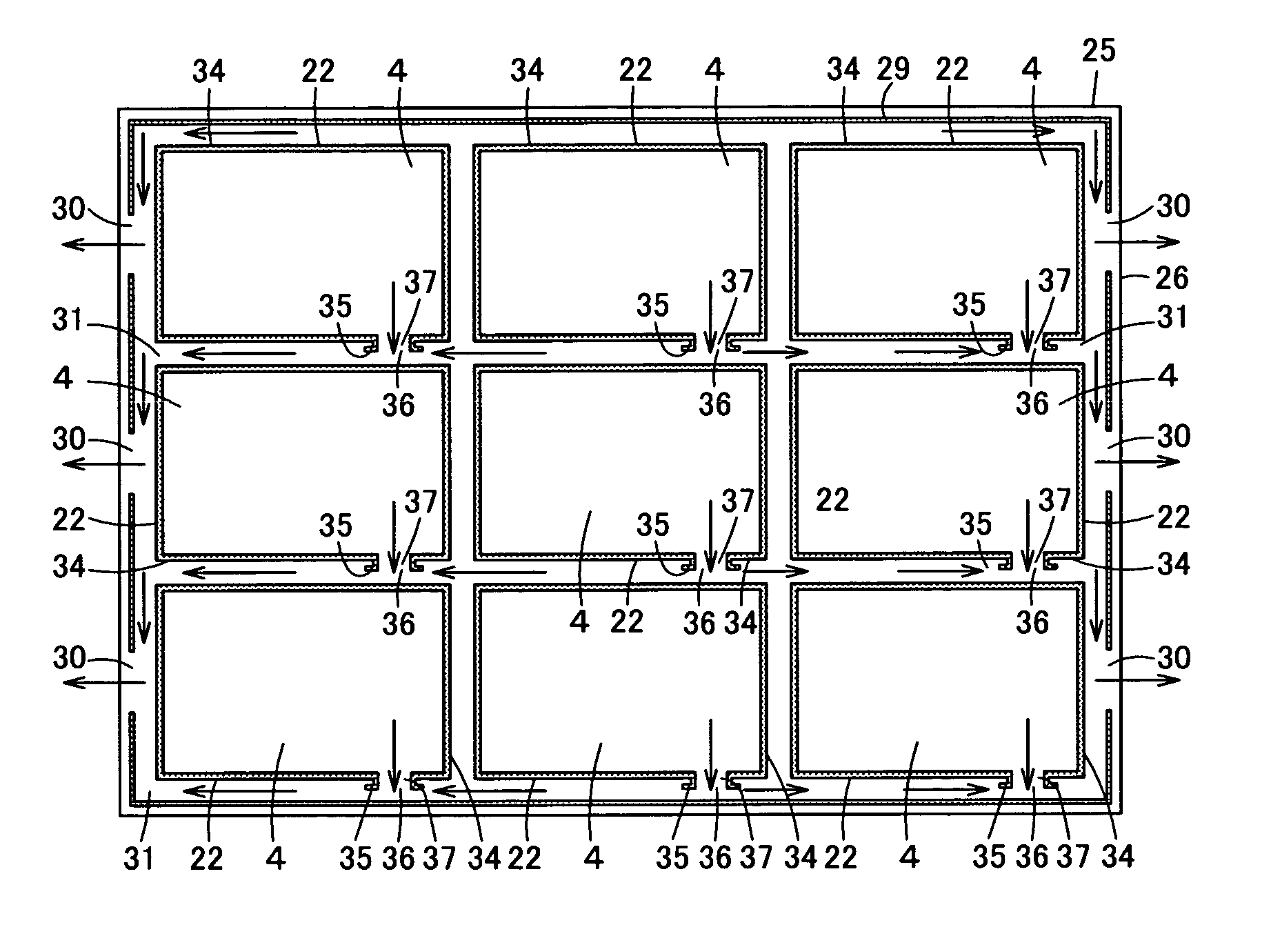
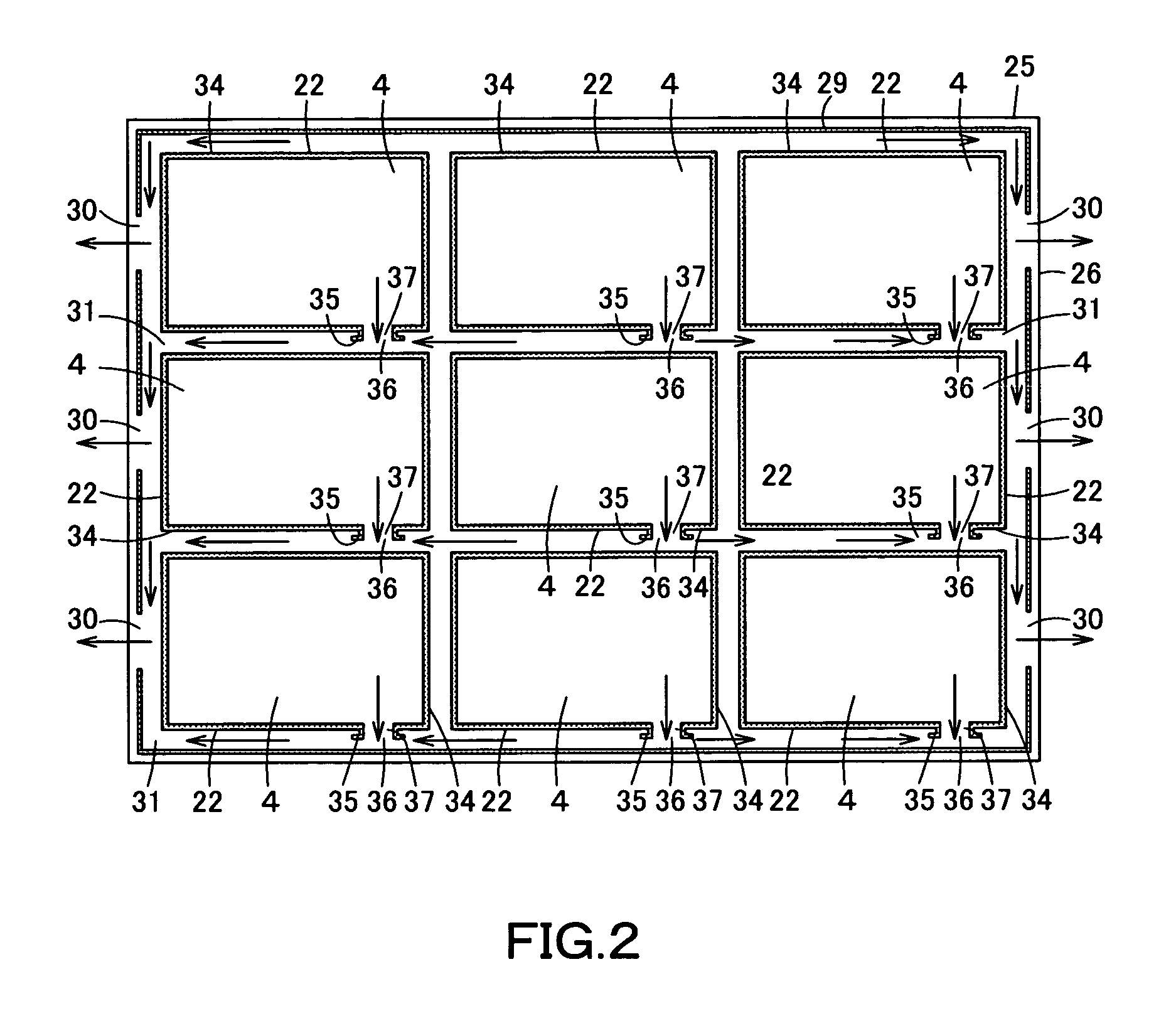
[0017]The construction of a first embodiment of a liquid crystal display device according to the present invention will be described with reference to FIGS. 1 to 4.

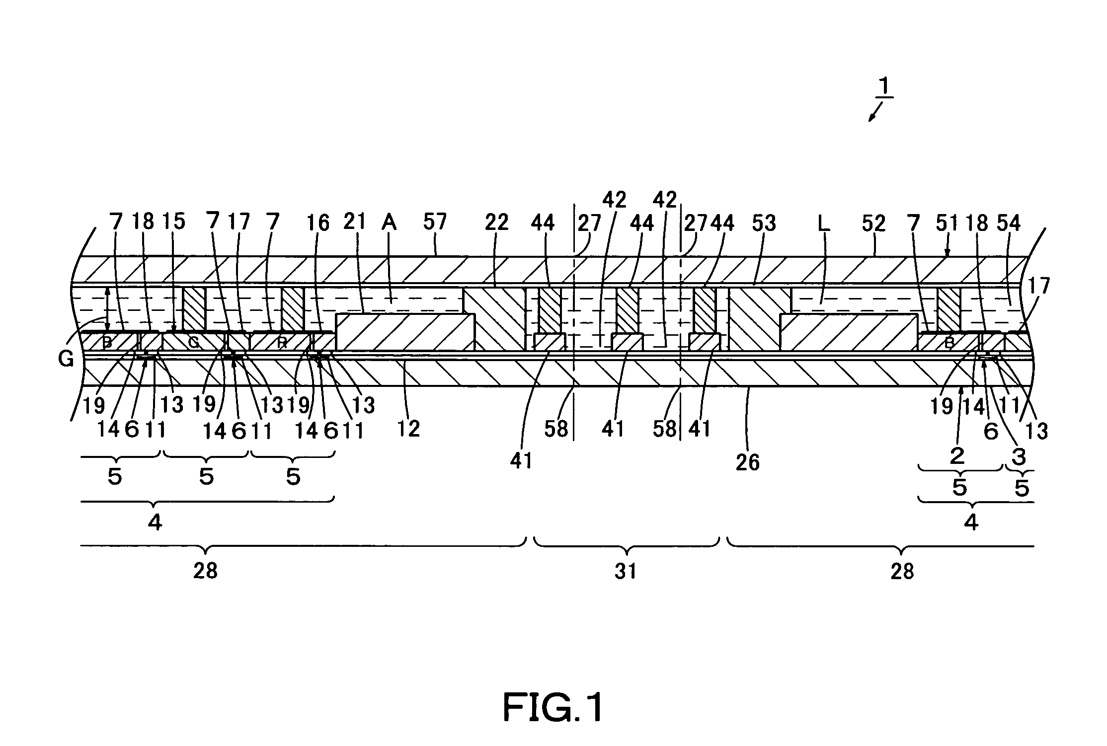
[0018]In FIGS. 1 to 4, 1 denotes a liquid crystal panel as a board device, and the liquid crystal panel 1 is a liquid crystal display element as a liquid crystal display device which can perform color image display. The liquid crystal panel 1 is equipped with a substantially rectangular flat plate array substrate 2 as a color filter substrate corresponding to a first substrate. Furthermore, as shown in FIG. 1, the array substrate 2 has a glass substrate 3 as a transparent insulating substrate formed of a substantially rectangular flat translucent plate insulating substrate having translucency.

[0019]An image display area 4 as a display pixel area corresponding to a rectangular image display area which can perform image display is provided at the center portion on the surface corresponding to one principal surface of the gl...


PUM

PropertyMeasurementUnit
widthaaaaaaaaaa
widthaaaaaaaaaa
temperatureaaaaaaaaaa

Abstract

Main body groove portions are formed along the longitudinal direction on the surface of a spacer height adjusting layer provided on a margin area of a large-size glass substrate. The cross-sectional area between seal materials between image display areas is increased. An air discharge efficiency from the inside of the image display area between the large-size glass substrates can be enhanced. The air discharge from the inside of the imaged is play area can be further reliably and readily performed. Liquid crystal composition can be readily injected from a liquid crystal injection port into the image display area. The time required to inject the liquid crystal into the image display area can be shortened. The productivity of liquid crystal panels can be enhanced.

Description

INCORPORATION BY REFERENCE[0001]The present application claims priority under 35 U.S.C. §119 to Japanese Patent Application No. 2005-302966 filed on Oct. 18, 2005. The content of the application is incorporated herein by reference in its entirety.FIELD OF THE INVENTION[0002]The present invention relates to a board device and a liquid crystal display device in which a second substrate is arranged in counterposition to a first substrate.BACKGROUND OF THE INVENTION[0003]A liquid crystal display device as this type of board device is equipped with an array substrate and a counter substrate each of which has an orientation film, and the array substrate and the counter substrate are disposed so that the orientation films thereof are in counterposition to each other. A liquid crystal layer is sandwiched in the cell gap between the orientation film of the array substrate and the orientation film of the counter substrate. A seal material and a sealing material are disposed on the peripheral ...

Claims


Application Information

Patent Timeline
Patent Type & Authority Patents(United States)
IPC IPC(8): G02F1/1339
CPCG02F1/1339G02F1/1341G02F1/133351
Inventor MANABE, ATSUYUKI
Owner JAPAN DISPLAY CENTRAL CO LTD
Why Eureka
Try Eureka