System including integrated circuit structures formed in a silicone ladder polymer layer

a technology of silicone ladder and integrated circuit, which is applied in the direction of semiconductor/solid-state device details, instruments, photomechanical equipment, etc., can solve the problems of large striation, poor etching rate, and large striation, and achieve the effect of reducing striation and cd loss

Inactive Publication Date: 2009-06-09
MICRON TECH INC
View PDF18 Cites 3 Cited by
  • Summary
  • Abstract
  • Description
  • Claims
  • Application Information

AI Technical Summary

Benefits of technology

[0008]The present invention provides a method of forming integrated circuit structures, such as capacitors, conductive plugs and other structures, formed within contact openings of a photosensitive silicone ladder polymer (PVSQ). The present invention further provides a method of forming a contact opening in a layer of photosensitive silicone ladder polymer (PVSQ) with reduced striations and CD loss.

Problems solved by technology

During photolithography, problems arise because high resolution submicrometer images in photoresist require shallow depth of focus during exposure, but thick photoresist patterns are required because of the poor etch rate between the photoresist and the underlying semiconductor layer.
As a consequence, irregular topographies, distorted images, large striations and uncontrolled increases in the size of the contact openings or holes, known as CD losses, occur during the exposure of the photoresist layer.
When two discontinuities are formed in adjacent contact openings, the integrated circuit suffers a loss in critical dimension (CD loss), which is critical especially in the sub-quarter micron regime.
As a result of the irregular contact openings, an unwanted and uncontrolled increase in the diameter of the contact openings may also result.
Thus, in addition to the loss in critical dimension, electrical contacts may also become unreliable.

Method used


Image

  • System including integrated circuit structures formed in a silicone ladder polymer layer
  • System including integrated circuit structures formed in a silicone ladder polymer layer
  • System including integrated circuit structures formed in a silicone ladder polymer layer

Examples


Embodiment Construction

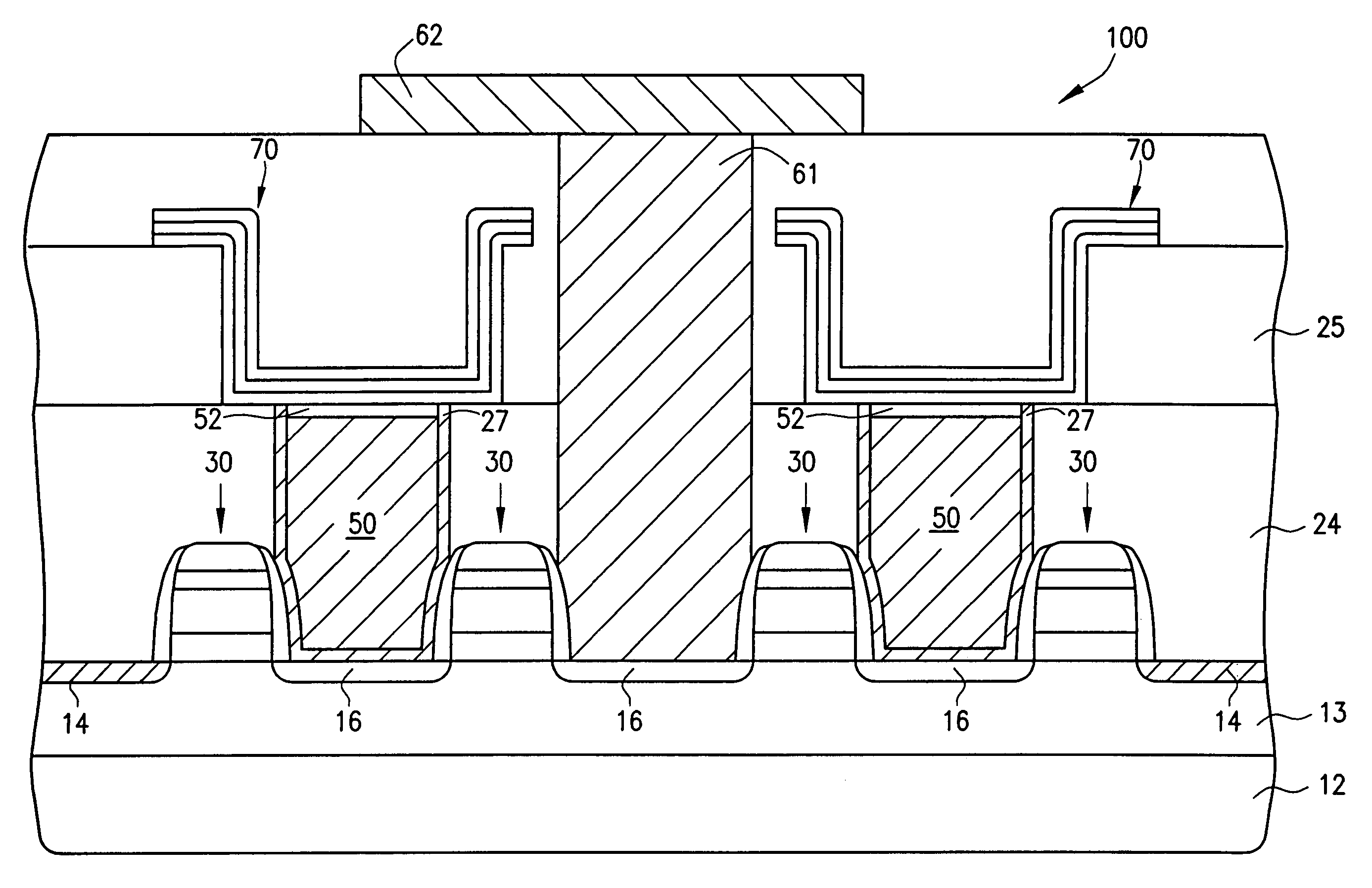
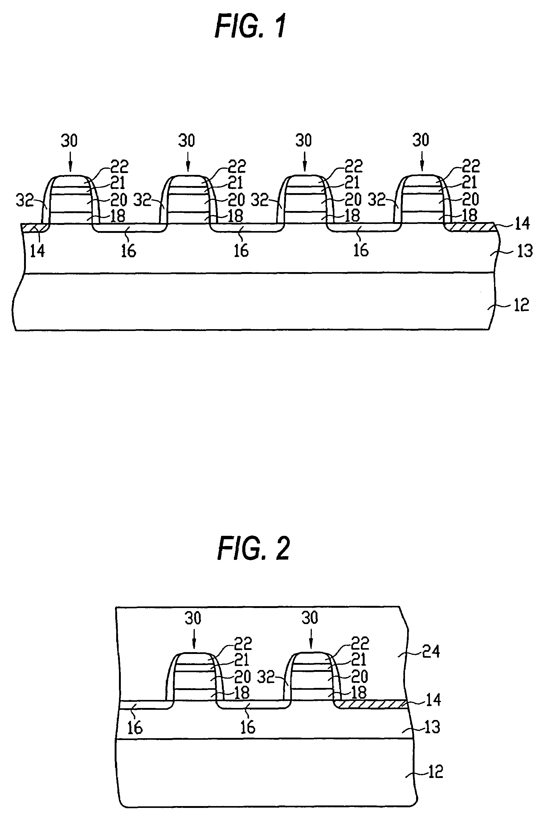
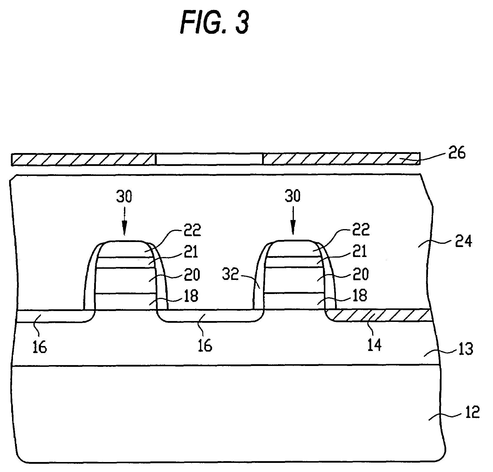
[0024]In the following detailed description, reference is made to various exemplary embodiments for carrying out the invention. These embodiments are described with sufficient detail to enable those skilled in the art to practice the invention, and it is to be understood that other embodiments may be employed, and that structural, electrical and process changes may be made, and equivalents substituted, without departing from the invention. Accordingly, the following detailed description is exemplary and the scope of the present invention is not limited by the detailed description but is defined solely by the appended claims.

[0025]The terms “wafer” or “substrate” used in the following description may include any semiconductor-based structure that has a silicon surface. Wafer and structure must be understood to include silicon-on insulator (SOI), silicon-on sapphire (SOS), doped and undoped semiconductors, epitaxial layers of silicon supported by a base semiconductor foundation, and o...


PUM

PropertyMeasurementUnit
thicknessaaaaaaaaaa
thicknessaaaaaaaaaa
temperatureaaaaaaaaaa

Abstract

A method of forming integrated circuit structures, such as capacitors and conductive plugs, within contact openings formed in a photosensitive silicone ladder polymer (PVSQ) is disclosed. Contact openings with reduced striations and CD loss are formed in a photosensitive silicone ladder polymer (PVSQ) layer by patterning the PVSQ film employing a photomask with a predefined pattern, exposing the PVSQ film to i-line, developing the exposed PVSQ film in a mixture of anisole / xylene in a ratio of about 1:2 for about 30 seconds, and subsequently optionally annealing the undeveloped PVSQ film at a temperature of about 300° C. to about 600° C.

Description

CROSS REFERENCE TO RELATED APPLICATIONS[0001]The present application is a divisional of U.S. application Ser. No. 10 / 101,750, filed on Mar. 21, 2002, now U.S. Pat. No. 7,091,131 the disclosure of which is herewith incorporated by reference in its entirety.FIELD OF THE INVENTION[0002]The present invention relates to the field of semiconductor integrated circuits and, in particular, to a novel method of forming contact openings and respective integrated circuit structures in a photosensitive silicone ladder polymer insulating layer.BACKGROUND OF THE INVENTION[0003]Semiconductor integrated circuits with high device density require the patterning of closely spaced submicrometer lines in semiconductors materials to form submicron geometries such as small area emitters for bipolar transistors, short gates for field effect transistors and narrow interconnection lines between devices. The formation of such polysilicon, metal or insulator structures typically requires definition of the locat...

Claims


Application Information

Patent Timeline
Patent Type & Authority Patents(United States)
IPC IPC(8): H01L29/92G03F7/075H01L21/027H01L21/285H01L21/311H01L21/312H01L21/60H01L21/768
CPCG03F7/0757H01L21/0273H01L21/28562H01L21/31138H01L21/3121H01L21/76802H01L21/76843H01L21/76849H01L21/76897H01L21/7687H01L21/022H01L21/02126
Inventor RASMUSSEN, ROBERT
Owner MICRON TECH INC
Why Eureka
Try Eureka