

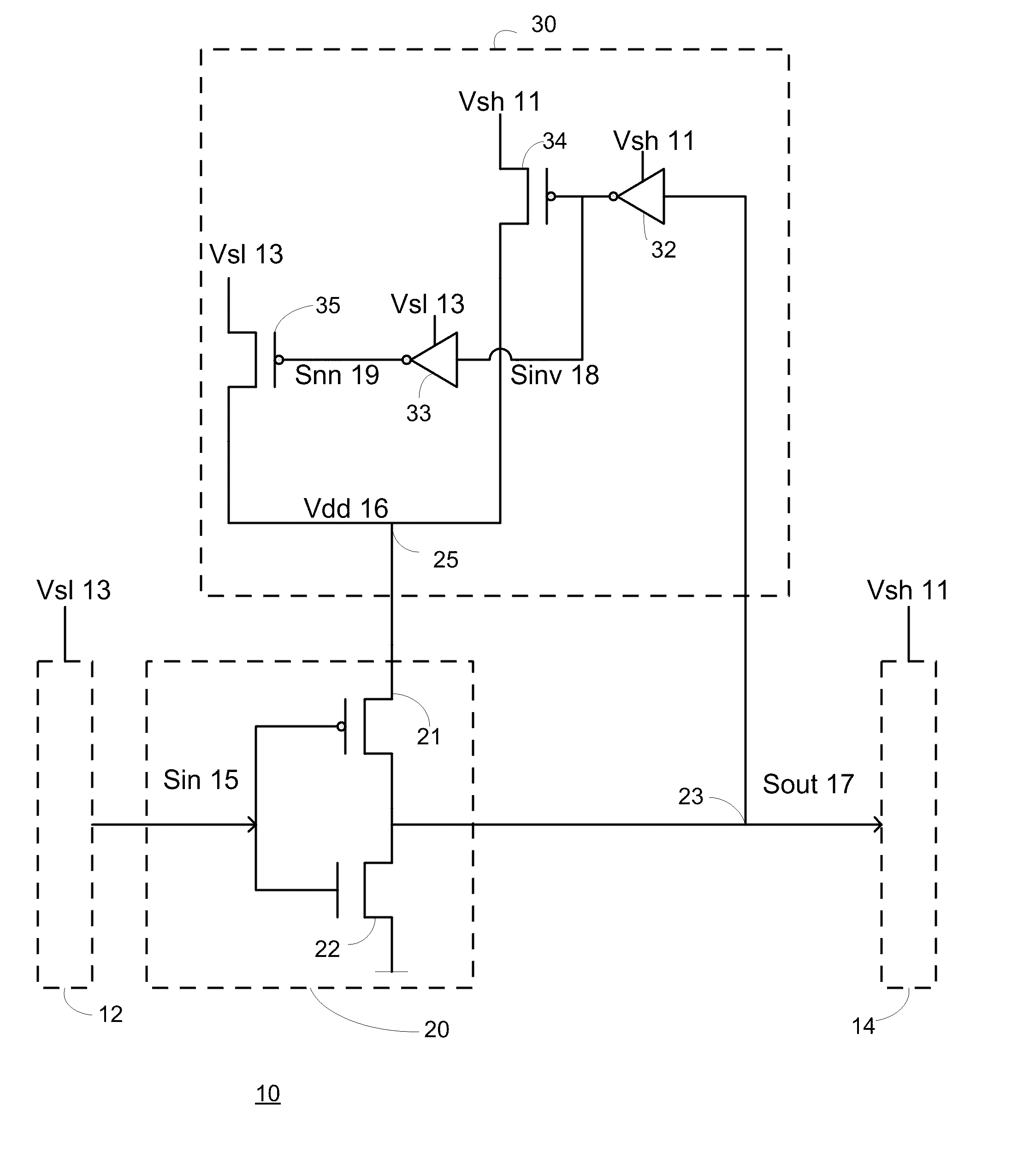
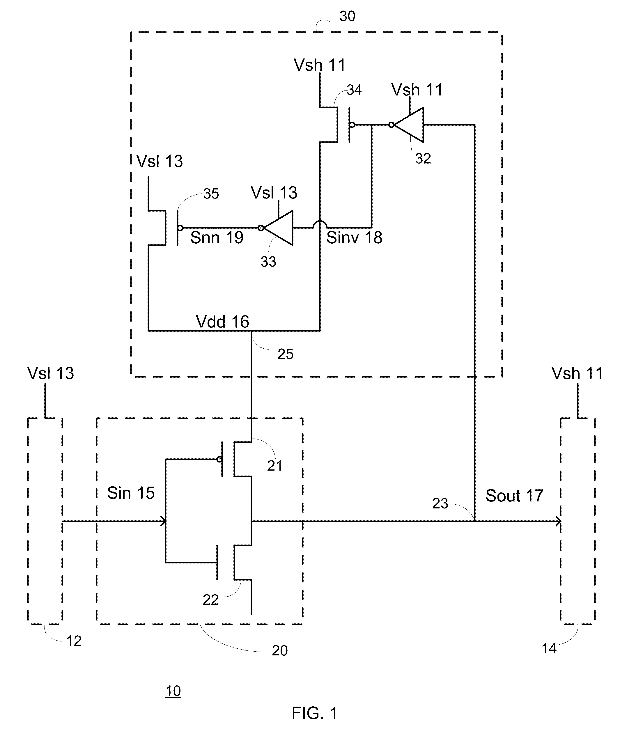
Scheme of level shifter cell
a level shifter and cell technology, applied in the direction of logic circuits, logic circuit coupling/interface arrangements, pulse techniques, etc., can solve the problems of delay and slow speed of the prior art level shifter
- Summary
- Abstract
- Description
- Claims
- Application Information
AI Technical Summary
Problems solved by technology
Method used
Image

Examples
Embodiment Construction
[0011]Although the invention is described herein with reference to specific embodiments, various modifications and changes can be made without departing from the scope of the present invention as set forth in the claims below.
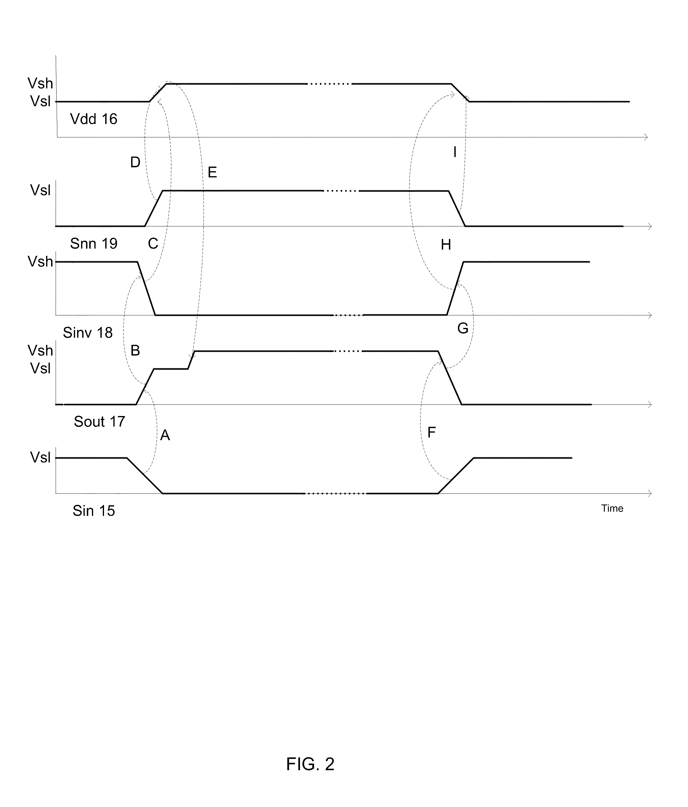
[0012]An efficient voltage level conversion can be based upon the following assumptions: (i) complementary MOS (CMOS) transistors (such as at least one PMOS transistor and at least one NMOS transistor) are included in a logic circuit and especially at its output stage; (ii) a low level output signal (also referred to as ‘0’, ground, substantially zero volts or a reference voltage, rail voltage) can be outputted by the logic circuit when the NMOS transistor is in a conductive mode and the PMOS transistor is in a non conductive mode, and this can occur (relatively quickly) by providing a high voltage level (for example of about a low level supply voltage or about a high level supply voltage) to the gates of the PMOS transistor and the NMOS transistor; and (iii) a...
PUM
 Abstract
Description
Claims
Application Information