Conventional
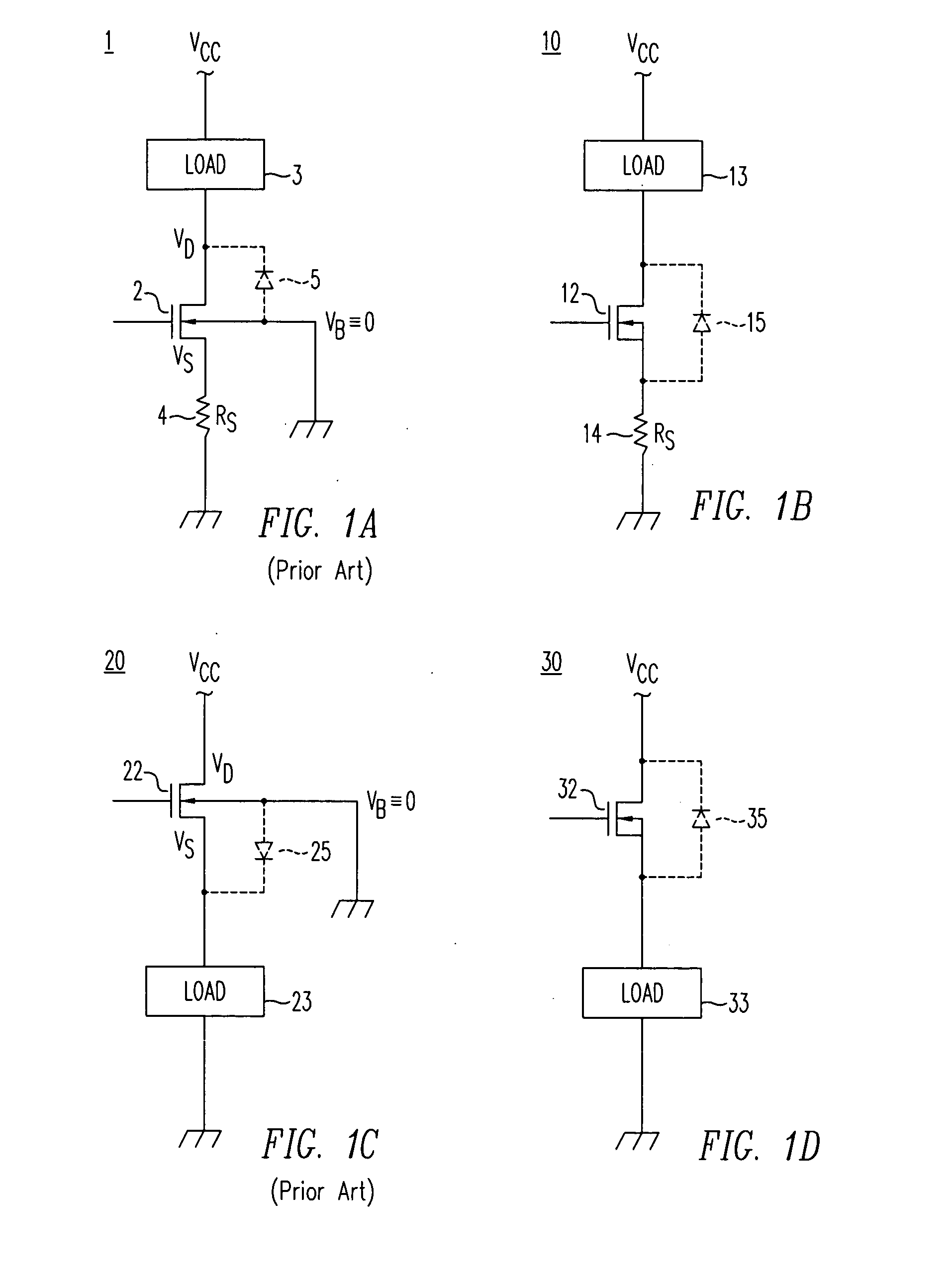
CMOS fabricated in P-type substrate material does not facilitate complete isolation of its devices since every P-type well forming the body (back-gate) of NMOS transistors is shorted to the substrate potential, typically the most negative on-chip potential.
High temperature
processing causes a redistribution of
dopant atoms in the substrate and epitaxial
layers, causing unwanted tradeoffs and compromises in the manufacturing of dissimilar devices fabricated using one common process.
Moreover, the high-temperature diffusions and
epitaxy employed in epi-JI processes are generally incompatible with the large
wafer diameters and advanced low-temperature processing equipment common in submicron
CMOS fabs.
The
voltage differential between source and body causes a number of problems.
A high threshold in turn increases on-resistance while lowering
saturation current, adversely impacting switch performance.
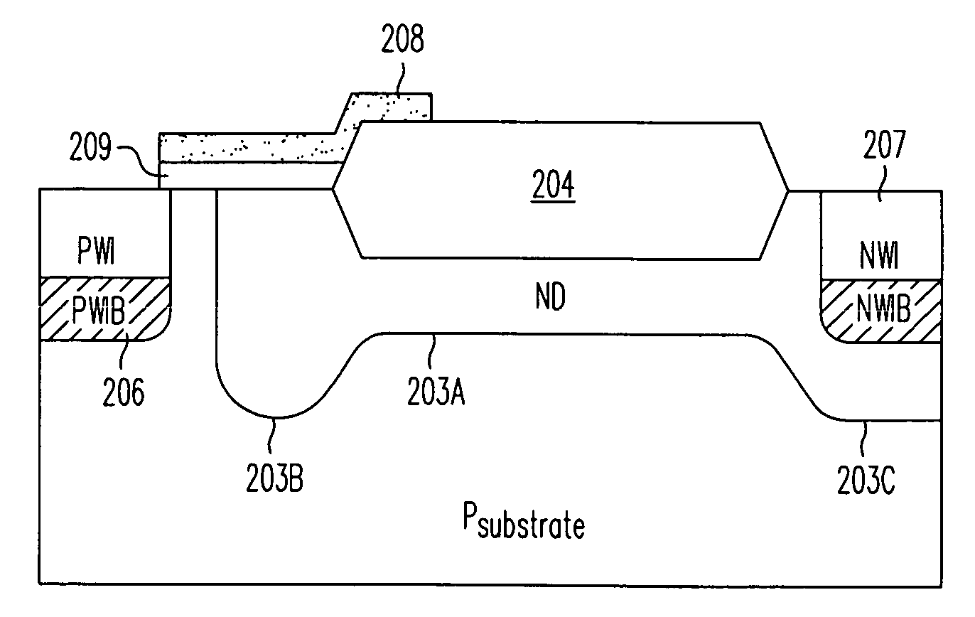
Integration of a source body short into a large area NMOS, while common in discrete power devices, requires isolation of the P-type body from the P-type substrate in integrated form, something conventional CMOS cannot offer.
Processes offering such isolation are complex to manufacture, often requiring high temperature fabrication steps.
The resulting body effect causes the threshold of NMOS 22 to increase substantially, making it difficult to provide adequate gate drive to achieve a low on-resistance without damaging the
thin gate oxide of NMOS 22.
Integration of a source body short into a large area NMOS, while common in discrete power devices, requires isolation of the P-type body from the P-type substrate in integrated form, something conventional CMOS cannot offer.
Processes offering such isolation are complex to manufacture, often requiring high temperature fabrication steps.
Without isolation, such a device cannot be integrated monolithically with other components or circuitry.
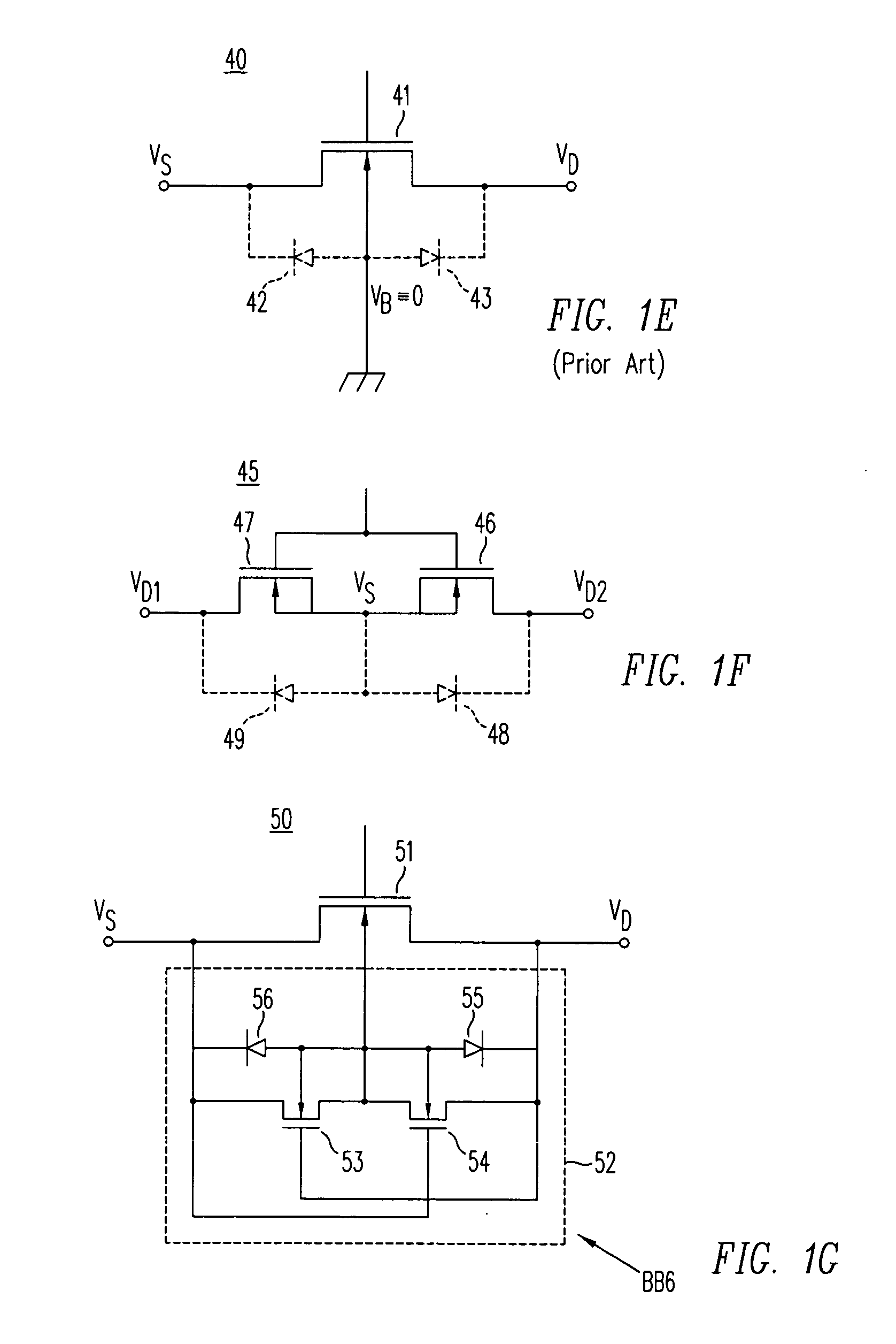
A
disadvantage of AC switch 45 is its high specific on-resistance, i.e. a large RDSA, since the two series connected transistors exhibit additive resistances.
Aside from the need to integrate NMOS devices with isolated source body shorts, another limitation of conventional CMOS is its inability to prevent undesirable
snapback breakdown effects in
MOSFET operation, particularly in NMOS transistors.
Because of
surface charge and other unavoidable surface effects, however, the
equipotential lines do not spread themselves uniformly, but instead “bunch up” near the gate edge resulting an a locally higher
electric field at the end of the drift region.
First the electrons are accelerated to high energies relative to the
crystal, i.e. they become energetically “hot”, and may get swept into the
gate oxide damaging the
dielectric.
Moreover, the two
negative resistance effects can occur simultaneously, interacting in a complex and even unpredictable way.
If the drain is driven into avalanche at high currents while sustaining voltage BVDSS, it may suddenly collapse back to BVCER, causing the current to increase and destroying the device.
The other effect is that the parasitic NPN
gain is too great since there is not enough base charge in the lightly doped substrate.
The extra N− drift
doping may be added to optimize the tradeoff between breakdown and resistance but remains limited by
impact ionization effects where the gate juxtaposes the drift region.
The
diffusion, taking anywhere from 7 to 24 hours, requires high temperatures over 1050° C. and typically 1100° C. or higher, a process incompatible with many modern low-temperature fabrication facilities and large
wafer diameters.
The lateral
implant method is complex and undesirable for manufacturing since the
implant must be performed four times to cover all four gate orientations on a
wafer.
Rotating the wafer during implantation makes uniform implantation difficult.
Unfortunately such a profile means the surface electric field is higher than in the bulk away from the surface, not ideal for manufacturing robust avalanche-rugged devices.
The high temperature diffusions involved in DMOS body fabrication are further complicated by the steps needed to achieve full
electrical isolation of circuitry using epitaxial
junction isolation.
As described previously, the problem with conventional epitaxial and high-temperature processes and manufacturing methods used to fabricate, isolate, and integrate high-voltage devices is that each high temperature process causes
dopant redistribution affecting every high-voltage and low-voltage device.

