Device structures for a metal-oxide-semiconductor field effect transistor and methods of fabricating such device structures

a technology of metal oxide and semiconductor, applied in the direction of semiconductor devices, basic electric elements, electrical equipment, etc., can solve the problems of large number of fabrication steps, and difficulty in perfecting thick gate oxides in high-performance cmos,

Inactive Publication Date: 2009-07-16
GLOBALFOUNDRIES INC
View PDF48 Cites 182 Cited by
  • Summary
  • Abstract
  • Description
  • Claims
  • Application Information

AI Technical Summary

Benefits of technology

[0008]In another embodiment, a method is provided for fabricating a device structure on an insulating layer. The method includes forming a first semiconductor body having a first sidewall that extends toward the insulating layer and forming a second semiconductor body having a second sidewall that extends toward the insulating layer. The first semiconductor body is doped to form a source and a drain. A gate die

Problems solved by technology

Thick gate oxides may be difficult to perfect in high-performance CMOS because of the relatively small thickness of the SOI layer.
Moreover, integration of both low-voltage and high-voltage MOSFET devi

Method used


Image

  • Device structures for a metal-oxide-semiconductor field effect transistor and methods of fabricating such device structures
  • Device structures for a metal-oxide-semiconductor field effect transistor and methods of fabricating such device structures
  • Device structures for a metal-oxide-semiconductor field effect transistor and methods of fabricating such device structures

Examples


Embodiment Construction

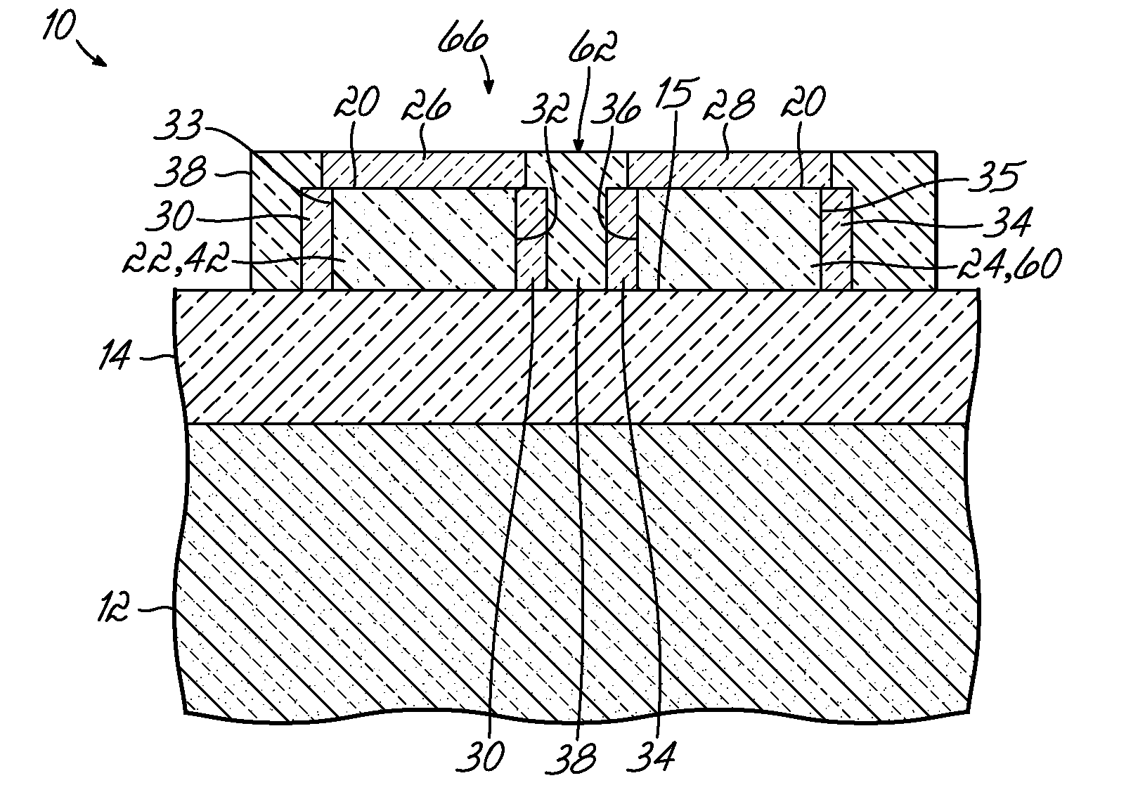
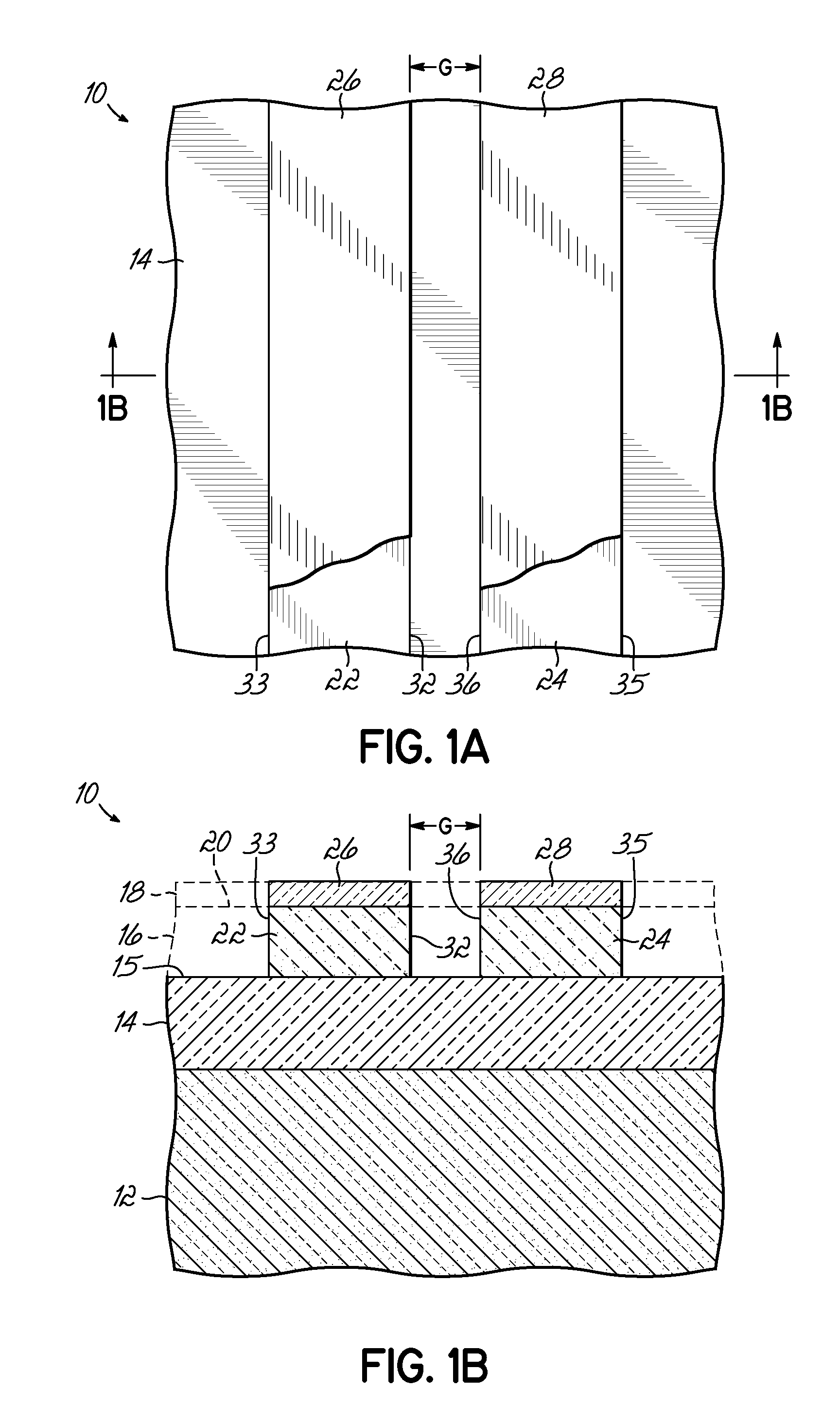
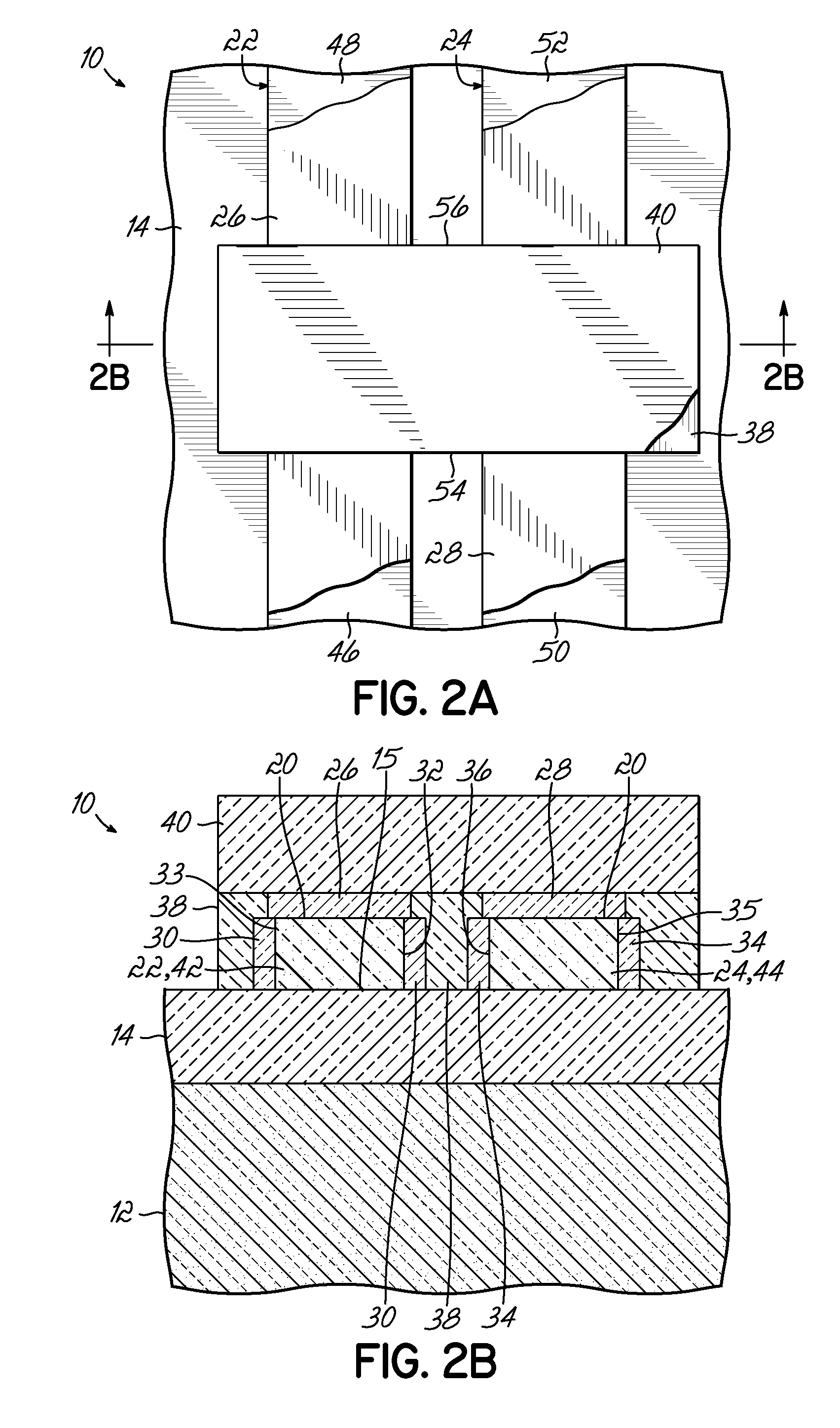
[0017]With reference to FIGS. 1A,B and in accordance with an embodiment of the invention, a semiconductor-on-insulator (SOI) substrate 10 includes a handle wafer 12, a buried insulating layer 14 formed of an insulating material such as silicon dioxide (e.g., SiO2), and an active semiconductor or SOI layer 16 separated from the handle wafer 12 by the intervening buried insulating layer 14. The SOI layer 16 is constituted by a single crystal or monocrystalline semiconductor material, such as silicon or a material that primarily contains silicon. The monocrystalline semiconductor material of the SOI layer 16 may contain a definite defect concentration and still be considered single crystal. The handle wafer 12 may also be constituted by a single crystal or monocrystalline semiconductor material, such as silicon, or another type of material. The SOI layer 16, which is considerably thinner than the handle wafer 12 and is in direct contact with a top surface 15 of the buried insulating la...


PUM


Abstract

Device structures for a metal-oxide-semiconductor field effect transistor (MOSFET) that is suitable for operation at relatively high voltages and methods of forming same. The MOSFET, which is formed using a semiconductor-on-insulator (SOI) substrate, includes a channel in a semiconductor body that is self-aligned with a gate electrode. The gate electrode and semiconductor body, which are both formed from the monocrystalline SOI layer of the SOI substrate, are separated by a gap that is filled by a gate dielectric layer. The gate dielectric layer may be composed of thermal oxide layers grown on adjacent sidewalls of the semiconductor body and gate electrode, in combination with an optional deposited dielectric material that fills the remaining gap between the thermal oxide layers.

Description

CROSS-REFERENCE TO RELATED APPLICATIONS[0001]This application is related to application Ser. No. ______, filed on even date herewith as Attorney Docket No. BUR920070211US1 and entitled “Device and Design Structures for Memory Cells in a Non-Volatile Random Access Memory and Methods of Fabricating Such Device Structures”.FIELD OF THE INVENTION[0002]The invention relates generally to semiconductor device fabrication and, in particular, to device structures for a metal oxide semiconductor field effect transistor (MOSFET) and methods for fabricating such device structures.BACKGROUND OF THE INVENTION[0003]Complementary metal-oxide-semiconductor (CMOS) technology is used in microprocessors, static random access memories, and other types of digital logic integrated circuits and analog integrated circuits. Generally, CMOS technology relies on complementary and symmetrical pairs of p-type and n-type metal oxide semiconductor field effect transistors (MOSFETs) to implement logic functions. Co...

Claims


Application Information

Patent Timeline
IPC IPC(8): H01L27/12H01L21/782
CPCH01L21/84H01L29/785H01L29/66795H01L27/1203
Inventor ABADEER, WAGDI W.CHATTY, KIRAN V.GAUTHIER, JR., ROBERT J.RANKIN, JED H.SHI, YUNTONTI, WILLIAM R.
Owner GLOBALFOUNDRIES INC
Why Eureka
Try Eureka