Organic light emitting display device

a light-emitting display and organic technology, applied in the direction of organic semiconductor devices, radio frequency controlled devices, instruments, etc., can solve the problems of easy deterioration of tfts performance, easy mass production, and easy large-scale production, so as to minimize the change in an electrical property of tfts

Active Publication Date: 2009-06-23
SAMSUNG DISPLAY CO LTD
View PDF6 Cites 5 Cited by
  • Summary
  • Abstract
  • Description
  • Claims
  • Application Information

AI Technical Summary

Benefits of technology

[0011]Accordingly, it is an aspect of the present invention to provide an organic light emitting display device in which channel regions of thin film transistors (TFTs) formed on a flexible substrate make a predetermined angle with the direction in which the substrate is bent so that a change in an electrical property of the TFTs can be minimized.

Problems solved by technology

Insulating substrates such as glass and quartz used for forming the above-described TFTs are fragile and heavy such that they cannot be easily made large and thus cannot be easily mass-produced.
However, since the film-shaped plastic substrate is vulnerable to heat and is sensitive to change in temperature, when the TFTs are formed on the film-shaped plastic substrate, the TFTs must be manufactured at a low temperature.
Therefore, when the TFTs are formed on the film-shaped plastic substrate, the performance of the TFTs may deteriorate more easily as compared with the case in which the TFTs are formed on a glass substrate.

Method used


Image

  • Organic light emitting display device
  • Organic light emitting display device
  • Organic light emitting display device

Examples


first embodiment

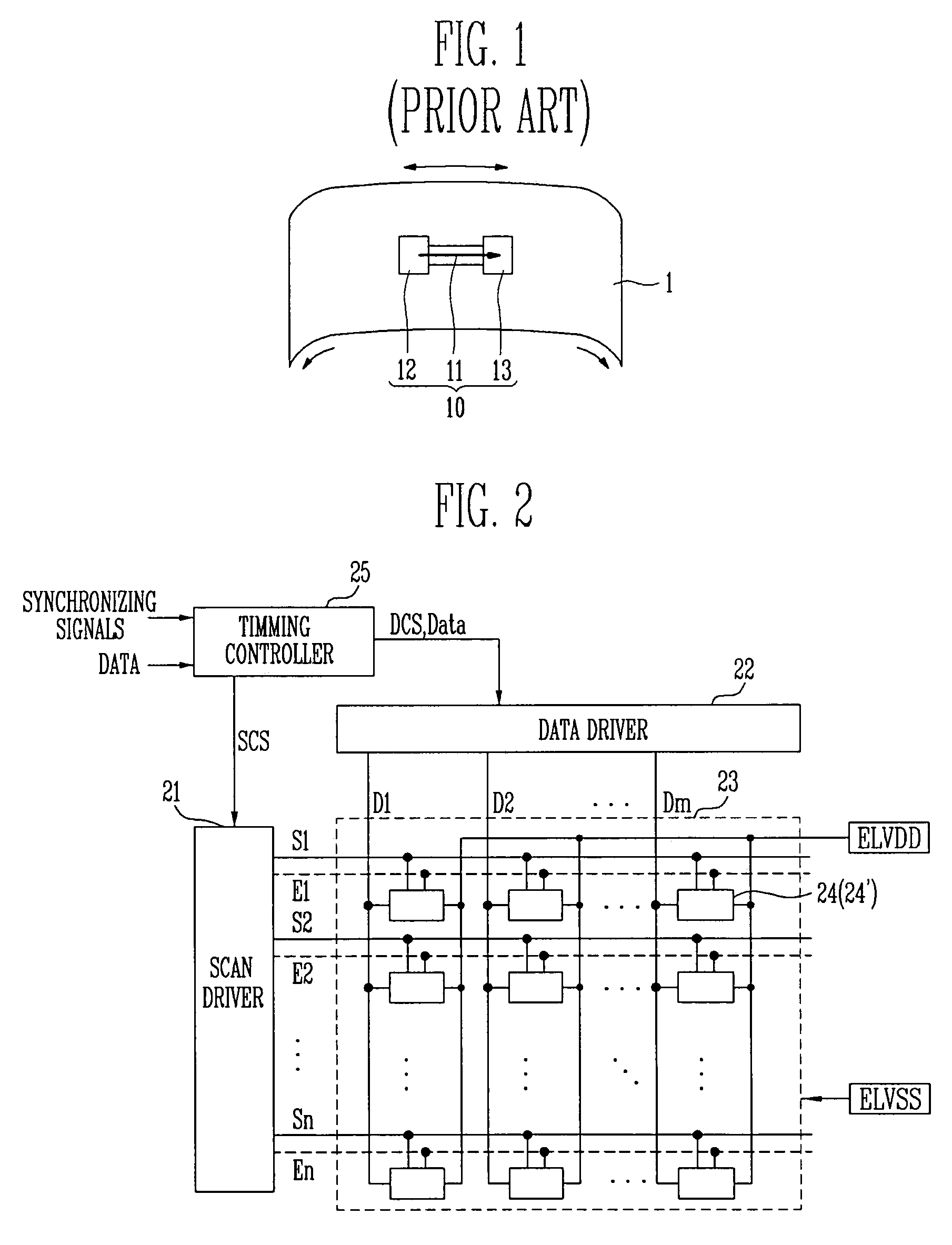
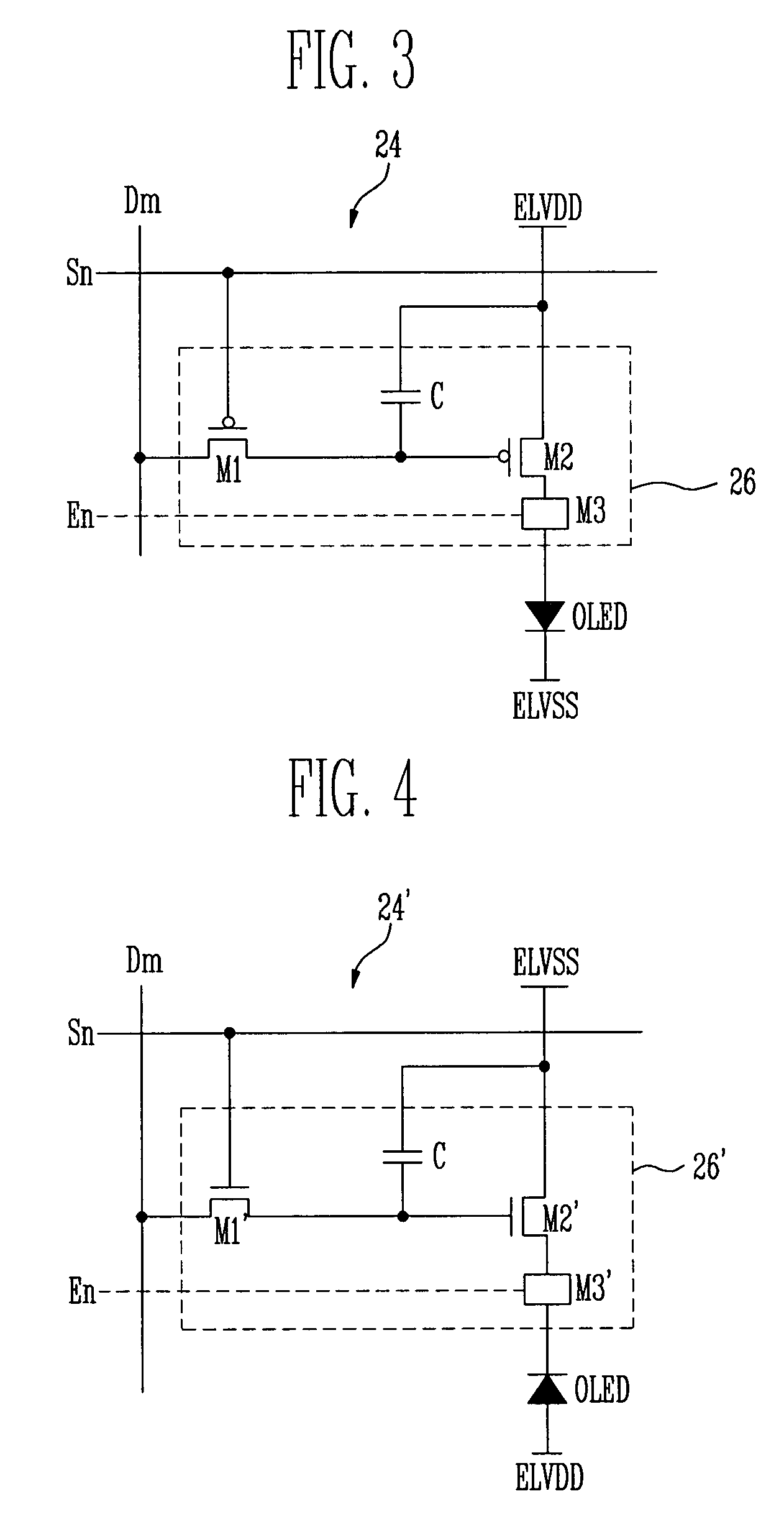
[0036]FIG. 3 illustrates a pixel 24 illustrated in FIG. 2. In FIG. 3, for convenience sake, the pixel 24 connected to the nth scan line Sn and the mth data line Dm is illustrated.

[0037]Referring to FIG. 3, the pixel 24 according to the first embodiment of the present invention includes an organic light emitting diode (OLED), and a pixel circuit 26 connected to the OLED, the data line Dm, the emission control line En, and the scan line Sn to emit light from the OLED. An anode electrode of the OLED is connected to the pixel circuit 26, and a cathode electrode of the OLED is connected to the second power source ELVSS. The OLED generates light corresponding to the current supplied from the pixel circuit 26.

[0038]The pixel circuit 26 includes a second pixel TFT M2 connected between the first power source ELVDD and the OLED; a first pixel TFT M1 connected with the second pixel TFT M2, the data line Dm, and the scan line Sn; and a storage capacitor C connected between a gate electrode of t...

second embodiment

[0041]However, in the pixel 24′ NMOS pixel TFTs M1′ and M2′ are used. FIG. 5 is a block diagram illustrating the structure of a shift register.

[0042]As illustrated in FIG. 5, the shift register according to an embodiment of the present invention includes n stages ST1 to STn connected to a start pulse SP input line. Also, each of the n stages ST1 to STn is connected to three clock signal supply lines C selected from among four clock signal supply lines for supplying clock signals CLK1 to CLK4.

[0043]In the shift register illustrated in FIG. 5, the output lines of the n stages are connected to n row lines ROW1 to ROWn (e.g., scan lines S1, S2, S3, S4, . . . . Sn) included in a pixel array, respectively. Each of the stages inputs only three clock signals selected from among the four clock signals CLK1 to CLK4 whose phases are sequentially delayed. For example, when the first, third, and fourth clock signals CLK1, CLK3, and CLK4 are input to the first stage ST1, three clock signals CLK2...


PUM

PropertyMeasurementUnit
angleaaaaaaaaaa
angleaaaaaaaaaa
angleaaaaaaaaaa

Abstract

An organic light emitting display device including a flexible substrate and a plurality of thin film transistors (TFTs) formed on the substrate. The plurality of TFTs formed on the substrate include a pixel transistor for driving a pixel and a driver circuit transistor for driving a driver circuit, and a longitudinal direction of a channel region of the pixel transistor makes a first predetermined angle with a direction in which the substrate is bent. As such, it is possible to minimize a change in the electrical property of the TFTs formed on the flexible substrate and to thus reduce a change in the amount of current that flows in the channels of the TFTs.

Description

CROSS-REFERENCE TO RELATED APPLICATION[0001]This application claims priority to and the benefit of Korean Patent Application No. 10-2005-0065943, filed on Jul. 20, 2005, in the Korean Intellectual Property Office, the entire content of which is incorporated herein by reference.BACKGROUND[0002]1. Field of the Invention[0003]The present invention relates to an organic light emitting display device, and more particularly, to an organic light emitting display device capable of minimizing a change in an electrical property of a thin film transistor (TFT) formed on a flexible substrate when the flexible substrate is bent in one or more directions.[0004]2. Discussion of Related Art[0005]Recently, a technology has been developed for forming a thin film transistor (TFT) using a semiconductor layer formed on an insulating substrate. The TFTs are used for electronic devices such as an integrated circuit and an electro-optical device, and more particularly, are used as switching devices and dri...

Claims


Application Information

Patent Timeline
Patent Type & Authority Patents(United States)
IPC IPC(8): G02F1/1343G02F1/1345H01L29/04H01L31/036H01L31/0376H01L31/20
CPCG02F1/13454H01L27/1214H01L29/78603H01L27/3244H01L2251/5338H01L27/1218H10K59/12H10K2102/311H01L27/12H01L29/78696
Inventor JEONG, JAE KYEONGKOO, JAE BONSHIN, HYUN SOOMO, YEON GONJEONG, JONG HANLEE, HUN JUNGKIM, SUNG JIN
Owner SAMSUNG DISPLAY CO LTD
Why Eureka
Try Eureka