
Method and apparatus for optical processing

a technology of optical processing and optical processing device, which is applied in the direction of logic circuits, pulse techniques, instruments using specific components, etc., can solve the problems of not being able to integrate optical processing devices on a single substrate or have the ability to interface with electronic systems with ease, and not being able to realize architectures

Inactive Publication Date: 2009-06-30
MACOM TECH SOLUTIONS HLDG INC
View PDF6 Cites 11 Cited by
  • Summary
  • Abstract
  • Description
  • Claims
  • Application Information

AI Technical Summary

Problems solved by technology

However, practical implementations of optical processors have not been realized.
Further, optical processing devices have not been shown to be integratable on a single substrate or to have the ability to interface with electronic systems with ease.
These difficulties are due to the fact that internal representations, realizations, and implementations of logic and arithmetic units utilizing interference characteristics, interconnections, and architectures have not been realized.

Method used


Image

  • Method and apparatus for optical processing
  • Method and apparatus for optical processing
  • Method and apparatus for optical processing

Examples


Embodiment Construction

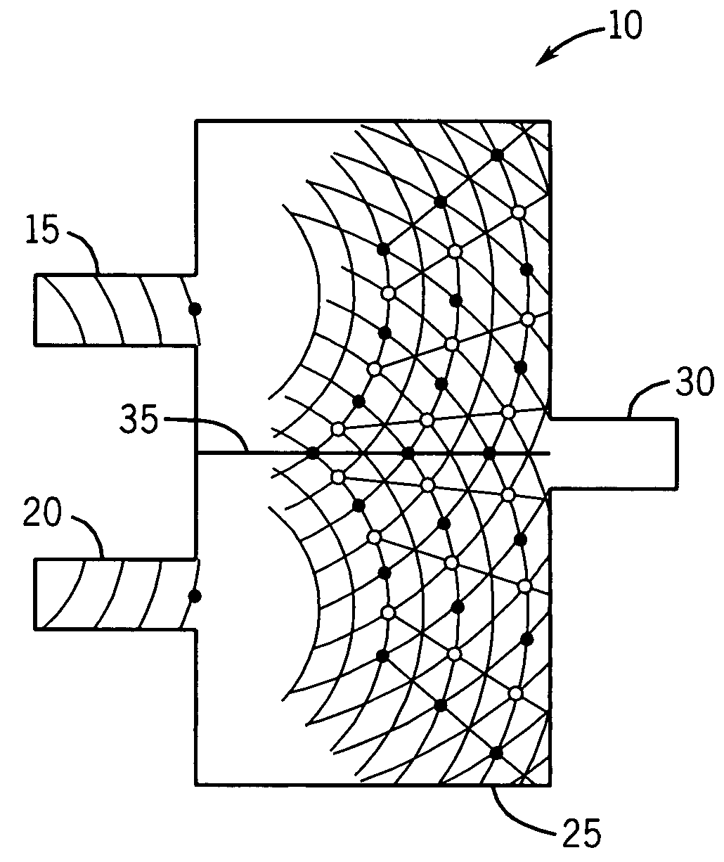
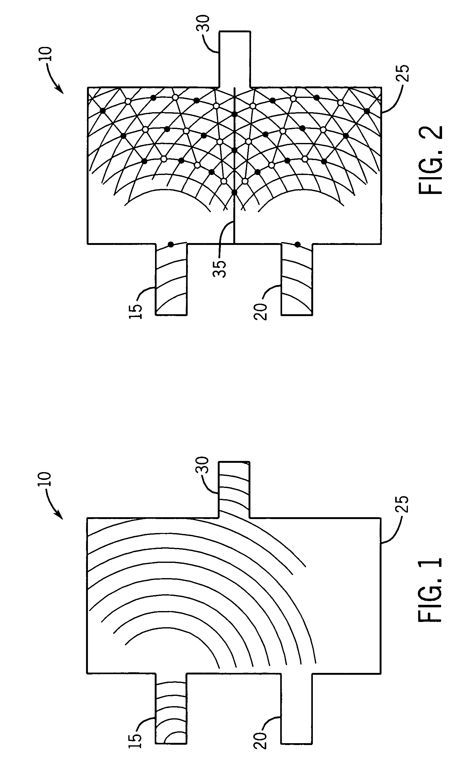
[0019]Referring now to FIG. 1, an exemplary embodiment of a NOT (inverter) gate 10 is depicted. Inverter gate 10 is a material patterned on a substrate, such as, but not limited to, a doped silicon or doped gallium arsenide material. Inverter gate 10 includes an optical bias input 15, optical bias input 15 configured to receive a constant light input or light bias (hereinafter, references made to light include any wavelength of electromagnetic radiation, including, but not limited to electromagnetic radiation in the visible spectrum). Inverter gate 10 further includes a second optical input 20 which selectively receives a light input. Further still, inverter gate 10 includes an interference region 25 in which light coming from inputs 15 and 20 is received. Inverter gate 10 also includes an optical output 30 that receives the optical output generated by interference region 25 based on inputs 15 and 20.

[0020]As depicted in FIG. 1, a bias light input is constantly received by bias ligh...


PUM

PropertyMeasurementUnit
wavelengthsaaaaaaaaaa
semiconductoraaaaaaaaaa
opticalaaaaaaaaaa

Abstract

An optical logic circuit is disclosed. The optical logic circuit is configured on a substrate of a first material. The optical logic circuit also has an optical layer which overlays the substrate layer and is at least partially configured of a second material. The optical layer is patterned to provide a plurality of optical pathways. At least one of the optical pathways transmits an optical bias and at least one optical pathway is configured to provide an optical input and at least one optical pathway is configured to provide an optical output. The optical pathways are configured to provide a Boolean logic output based on the at least one optical input.

Description

FIELD OF THE INVENTION[0001]The invention relates to optical computing devices. In particular, the invention relates to hardware implementations of optical computing logic gates. The optical logic gates are configured to be used in optical processing devices.BACKGROUND OF THE INVENTION[0002]Optical processors function based on the action of photons in an optical circuit. The use of optical processors provide faster computation times and immunity from electromagnetic interference when compared to conventional electronic processors. However, practical implementations of optical processors have not been realized. Optical processing devices have heretofore not been miniaturized, easily mass produced, made reliable and designed to consume low power. Further, optical processing devices have not been shown to be integratable on a single substrate or to have the ability to interface with electronic systems with ease. These difficulties are due to the fact that internal representations, real...

Claims


Application Information

Patent Timeline
Patent Type & Authority Patents(United States)
IPC IPC(8): G02F3/00G02B6/00
CPCG02B6/125G02B6/2813G02F3/00G02B2006/12145G02B2006/12159
Inventor GOLSHAN, KHOSROW
Owner MACOM TECH SOLUTIONS HLDG INC
Learn More