Display device

a display device and active matrix technology, applied in the field of active matrix display devices, can solve the problems of voltage drop, voltage drop, voltage drop, etc., and achieve the effect of voltage drop

Active Publication Date: 2009-07-07
SEMICON ENERGY LAB CO LTD
View PDF27 Cites 22 Cited by
  • Summary
  • Abstract
  • Description
  • Claims
  • Application Information

AI Technical Summary

Benefits of technology

[0015]Drop in voltage can be suppressed in such a manner, and thus a display devi

Problems solved by technology

As the length of a wiring is increased with enlargement of a display device, voltage drop occurs.
The voltage dr

Method used


Image

  • Display device
  • Display device
  • Display device

Examples


embodiment mode 1

[0025]An embodiment mode of the invention is described with reference to FIGS. 1A and 1B.

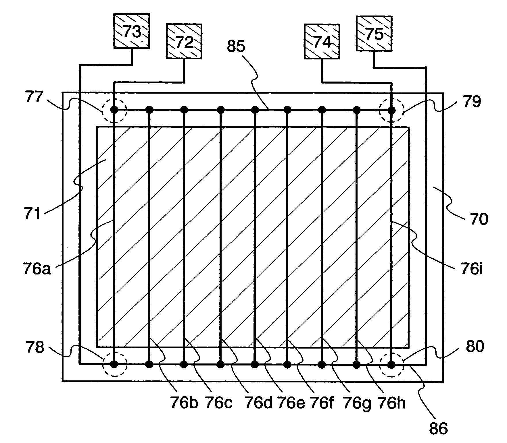
[0026]FIG. 1A is a pattern diagram showing current supply lines which are led out, among a plurality of wirings provided in the active matrix display device of the invention.

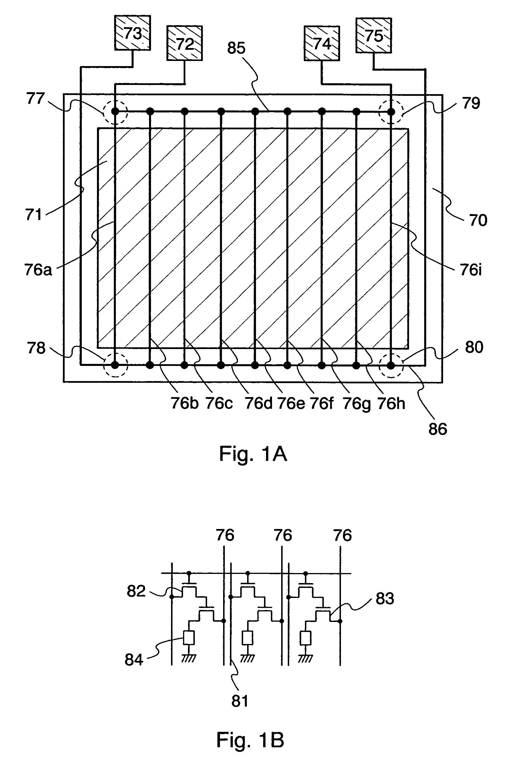
[0027]A pixel portion 71 formed on a substrate 70 comprises a plurality of pixels each having a switching transistor 82, a driving transistor 83 and a light emitting element 84 as shown in FIG. 1B. Further, reference numeral 81 denotes a source line and 76 denotes a current supply line in FIG. 1B. It is assumed in this embodiment mode that the light emitting element 84 in each pixel emits the same color light.

[0028]A plurality of current supply lines 76a to 76i provided on the substrate 70 extend in one direction and parallel to each other. The current supply lines 76a to 76i are connected to a wiring 85 which extends substantially perpendicular to the current supply lines 76a to 76i, and connected to a first current input t...

embodiment mode 2

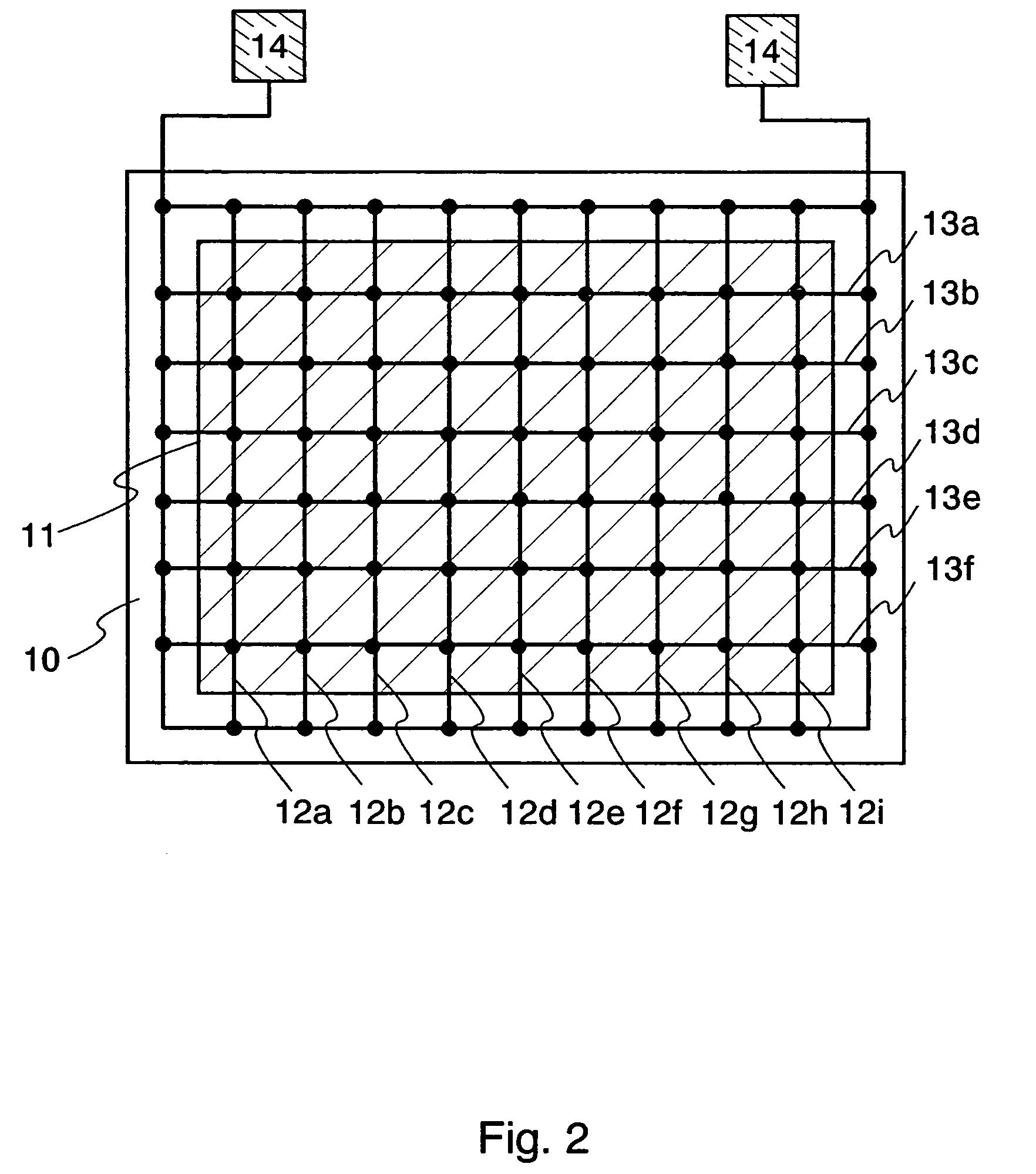
[0033]An embodiment mode of the invention is described with reference to FIGS. 2 and 3.

[0034]FIG. 2 is a pattern diagram showing current supply lines which are led out, among a plurality of wirings provided in the active matrix display device of the invention. FIG. 3 is a diagram showing a circuit configuration of the pixel portion of the display device shown in FIG. 2.

[0035]In FIG. 2, a pixel portion 11 formed on a substrate 10 comprises current supply lines 12a to 12i arranged in columns. Wirings 13a to 13f are arranged so as to intersect with the current supply lines 12a to 12i arranged in columns, and the wirings 13a to 13f are connected to the current supply lines 12a to 12i at intersections of the wirings 13a to 13f and the current supply lines 12a to 12i. Further, the current supply lines 12a to 12i are connected to current input terminals 14.

[0036]In FIG. 3, the pixel portion 11 of the display device comprises a plurality of current supply lines 90a to 90i arranged in a long...

embodiment

Embodiment 1

[0042]A display device using the invention is described with reference to FIGS. 4 to 7. Note that, the display device shown in this embodiment adopts the structures described in both Embodiment Modes 1 and 2. FIG. 7 is a diagram showing a circuit configuration of a pixel portion of the display device according to this embodiment.

[0043]FIG. 4 is a top plan view showing a part of a pixel portion of the display device according to the invention. FIG. 5 is a cross sectional view taken by cutting along a line A-A′ of FIG. 4, whereas FIG. 6 is a cross sectional view taken by cutting along a line B-B′ of FIG. 4.

[0044]A display device of this embodiment comprises a plurality of pixels using as a unit light emitting elements each of which emits red, green or blue light. Each of the pixels comprises a driving transistor 22 for driving the light emitting element, a switching transistor 20, an erasing transistor 21, a current supply line 28, source lines 25a and 25b, a first scan li...


PUM


Abstract

A display device in which the current load of wirings are distributed and display variations due to voltage drop are suppressed. An active matrix display device of the invention comprises a first current input terminal, a second current input terminal, and a plurality of current supply lines extending parallel to each other. Each current supply line is connected to a plurality of driving transistors in a line. One end of each current supply line is connected to the first current input terminal via a first wiring intersecting with the current supply lines, and the other end thereof is connected to the second current input terminal via a second wiring intersecting with the current supply lines. Accordingly, a current is supplied to each current supply line from both the first and the second current input terminals. The first and the second current input terminals are provided separately from each other.

Description

BACKGROUND OF THE INVENTION[0001]1. Field of the Invention[0002]The present invention relates to an active matrix display device, and more particularly, relates to a wiring structure of an active matrix display device comprising a light emitting element.[0003]2. Description of the Related Art[0004]In recent years, a large sized electro luminescence (abbreviated as EL hereinafter) display device has been developed with a view to entry into the television market.[0005]As the length of a wiring is increased with enlargement of a display device, voltage drop occurs. The voltage drop becomes a problem particularly in a current supply line for supplying a current to a light emitting element.[0006]This is because the voltage drop causes display variations since a voltage applied to an EL element varies among each region.SUMMARY OF THE INVENTION[0007]The invention provides a display device in which display variations due to voltage drop are suppressed by distributing the current load of wir...

Claims


Application Information

Patent Timeline
IPC IPC(8): G09G3/30G09G5/00
CPCG09G3/32G09G3/30H01L33/62G09G2320/0233G09G2300/0404G09G2320/0242G09G2330/02G09G2300/0809H01L2924/0002G09G2300/0426H01L2924/00H10K59/35H10K59/131H10K59/1213H01L27/124H01L27/15H01L27/156
Inventor TANADA, YOSHIFUMI
Owner SEMICON ENERGY LAB CO LTD
Why Eureka
Try Eureka