Semiconductor laser element
a laser element and semiconductor technology, applied in the direction of lasers, semiconductor lasers, laser optical resonator construction, etc., can solve the problems of reducing the kink level, degrading the temperature characteristic, and nonlinearity between, and achieve the effect of low aspect ratio and lowering the kink level
- Summary
- Abstract
- Description
- Claims
- Application Information
AI Technical Summary
Benefits of technology
Problems solved by technology
Method used
Image

Examples
embodiment 1
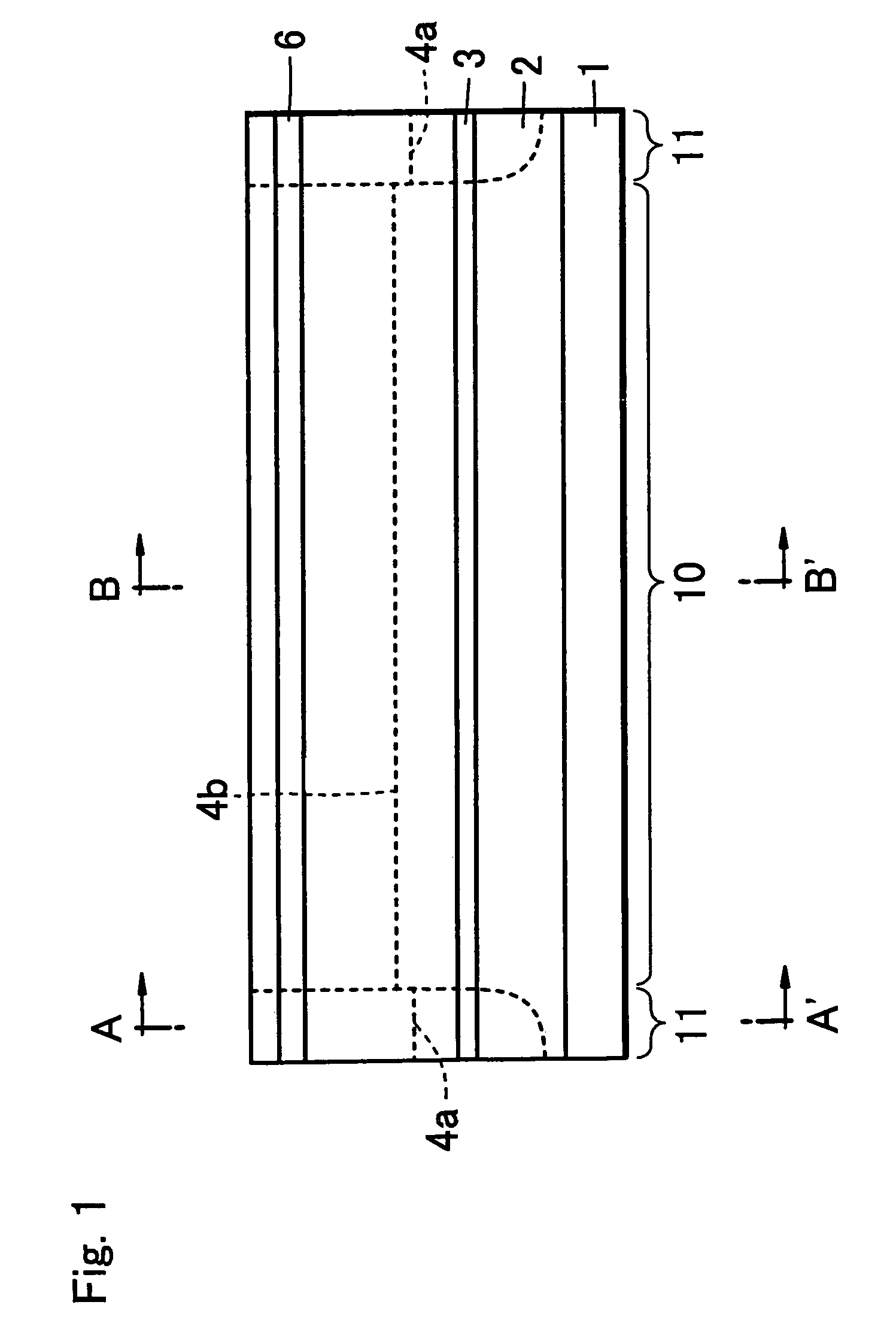
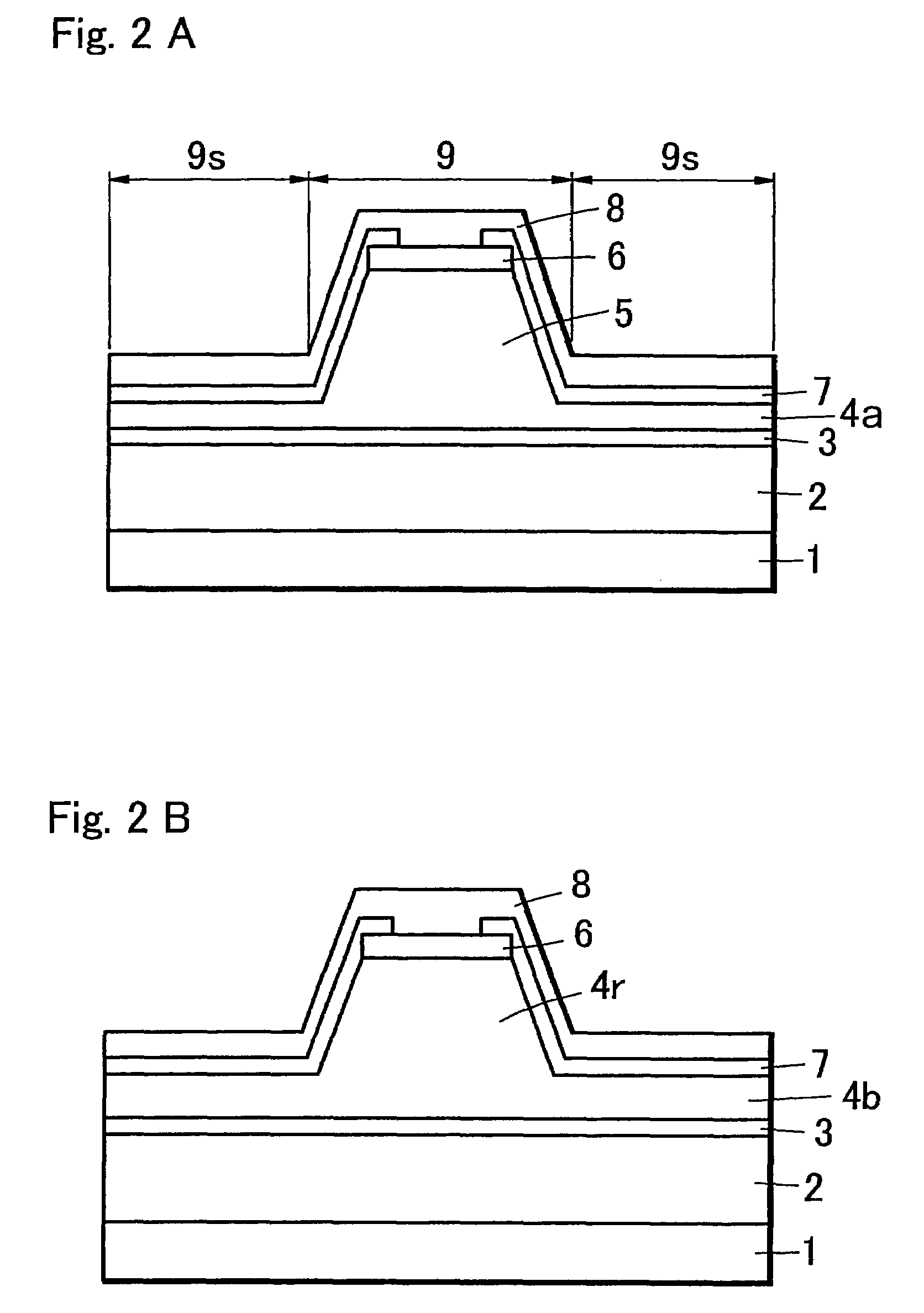
[0030]A semiconductor laser diode of the first embodiment related to the present invention is a ridge type semiconductor laser diode as shown in FIGS. 1, 2A and 2B, where FIG. 2A represents a sectional view of the semiconductor diode at line A-A′ at a window region 11 in FIG. 1, and FIG. 2B represents a sectional view of the semiconductor diode at line B-B′ at a gain region 10 in FIG. 1. The laser diode has a structure in which a ridge 9 is formed so that part of an upper cladding layer 4a, 4b are left behind on an active layer 3 on both sides of the ridge 9, and window regions 11, which are non-gain regions for preventing an optical damage, are formed at both ends (FIG. 1). As shown in FIGS. 1 and 2A, ridge 9 is formed by a portion 5 of the cladding layer 4a in the window region 11, and as shown in FIGS. 1 and 2B, and ridge 9 is formed by a portion 4r of the cladding layer 4b in the gain region 10. A layer 7 having an opening over a contact layer 6 that covers cladding layer 4A, 4b...
embodiment 2
[0055]A semiconductor laser element of the second embodiment related to the present invention is constructed in a similar manner to that in the first embodiment with the exceptions described below (FIG. 8).
[0056]Note that in FIG. 8, like symbols are attached to constituents similar to those in the first embodiment.
[0057]Distinction 1
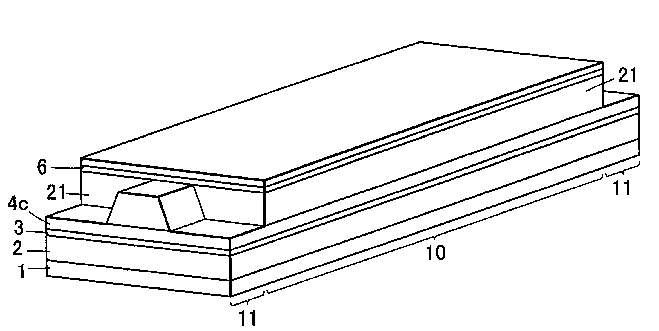
[0058]In the semiconductor laser diode of the second embodiment, a left upper cladding layer 4c with the same thickness is formed across a gain region 10 including window regions 11 on active layer on both sides of a ridge.
[0059]Distinction 2
[0060]A current blocking layer (buried layer) 21 is formed only on both sides of the ridge in the gain region 10.
[0061]In the semiconductor laser diode of the second embodiment with such a construction as well, an equivalent refractive index difference Δn11 between the ridge and portions on both sides thereof in non-gain regions (window regions) can be larger than an equivalent refractive index difference Δn10 betwee...
embodiment 3
[0064]A semiconductor laser element of the third embodiment related to the present invention is constructed in a similar manner to that in the second embodiment except that formed on both sides of a ridge in window regions 11 is a buried layer 21a made of a semiconductor material having a refractive index smaller than the current blocking layer 21 formed on both sides of the ridge in a gain region 10 (FIGS. 9A and 9B).
[0065]Note that in FIGS. 9A and 9B, like symbols are attached to constituents similar to those in the first or second embodiment.
[0066]In the semiconductor laser diode of the third embodiment with such a construction, an equivalent refractive index difference Δn11 between the ridge and portions on both sides thereof in non-gain regions (window regions) can be larger than an equivalent refractive index difference Δn10 between the ridge and portions on both sides thereof in the gain region 10.
[0067]Therefore, in the construction of the third embodiment as well, an FFPx c...
PUM
 Abstract
Description
Claims
Application Information
 - R&D
- Intellectual Property
- Life Sciences
- Materials
- Tech Scout
- Unparalleled Data Quality
- Higher Quality Content
- 60% Fewer Hallucinations
Browse by: Latest US Patents, China's latest patents, Technical Efficacy Thesaurus, Application Domain, Technology Topic, Popular Technical Reports.
© 2025 PatSnap. All rights reserved.Legal|Privacy policy|Modern Slavery Act Transparency Statement|Sitemap|About US| Contact US: help@patsnap.com