Method of correcting opaque defect of photomask using atomic force microscope fine processing device

a technology of atomic force microscope and processing device, which is applied in the direction of originals for photomechanical treatment, mechanical roughness/irregularity measurement, instruments, etc., can solve the problems of device defect to all of the transferred wafers, and achieve accurate correction, accurate detection of ending points, accurate detection of drift amoun

Active Publication Date: 2009-08-11
HITACHI HIGH TECH SCI CORP
View PDF3 Cites 4 Cited by
  • Summary
  • Abstract
  • Description
  • Claims
  • Application Information

AI Technical Summary

Benefits of technology

[0014]That is, returning scanning, which is used for only moving in the conventional scanning, is used for detecting an ending point and observing to acquire drift information. An opaque defect is processed by scanning with a high load or height fixed mode using a probe harder than a pattern material of a photomask at the time of going scanning; height information for every line is acquired by scanning with a low load or intermittent contact mode at the time of the returning scanning; and an ending point of a processing area is detected by this height information. In the next processing to the same area, a portion reaching to the ending point is not scanned by the scanning with the high load or height fixed mode, and only a portion not reaching to the ending point is scanned by the scanning with the high load or height fixed mode. Since an offset occurs between the going scanning and returning scanning due to the scanning directions according to processing conditions and observation conditions, height information of the returning scanning is corrected based on the offset amount so as to more accurately detect an ending point.
[0015]Further, information for every line acquired by the returning scanning with the low load or intermittent contact mode is reconfigured to make an image of the whole processing area, and information in the XY directions of the reconfigured image is used for correcting a drift. A typical pattern to be a drift marker and position information of a defect shape are compared between the previous reconfigured image and the new reconfigured image so as to calculate a drift amount in the processing area, and the area in which a drift is corrected is processed next time. Since an offset occurs between the going scanning and returning scanning due to the scanning directions according to processing conditions and observation conditions, XY information of the returning scanning is corrected based on the offset amount so as to more accurately detect a drift amount, and thus the returning scanning is more accurately corrected.
[0016]According to the present invention, when a defect of a mask are corrected using an atomic force microscope technique, a processing not having an over etch and grinding remainder and a high accuracy processing can be realized while increasing throughput.
[0017]That is, since the present invention effectively uses returning scanning conventionally used for only moving to the start point of a next line, total time for processing and observing can be shortened. Further, since the present invention detects a processing ending point by the height information of an image acquired by returning processing scanning, an ending point can be monitored for every processing scanning, and thus a processing having few over etches and grinding remainders can be performed.
[0018]Further, the present invention measures a drift amount by the XY information of an image, which is acquired by returning scanning with a low load or intermittent contact mode, and by comparing a pattern and position information of a defect with those of the previous processing, so as to correct a drift of the next processing. Thus, reducing processing accuracy by a drift can be prevented, and a high accuracy processing can be performed for a short time.

Problems solved by technology

As a mask is an original edition at the time of wafer transfer, if processing accuracy of a corrected portion is not enough or there is an over etch or grinding remainder, transfer property of the photomask is bad-influenced so as to cause a device defect to all of the transferred wafers.

Method used


Image

  • Method of correcting opaque defect of photomask using atomic force microscope fine processing device
  • Method of correcting opaque defect of photomask using atomic force microscope fine processing device
  • Method of correcting opaque defect of photomask using atomic force microscope fine processing device

Examples


Embodiment Construction

[0024]Hereinafter, examples of the present invention will be described in detail with reference to drawings.

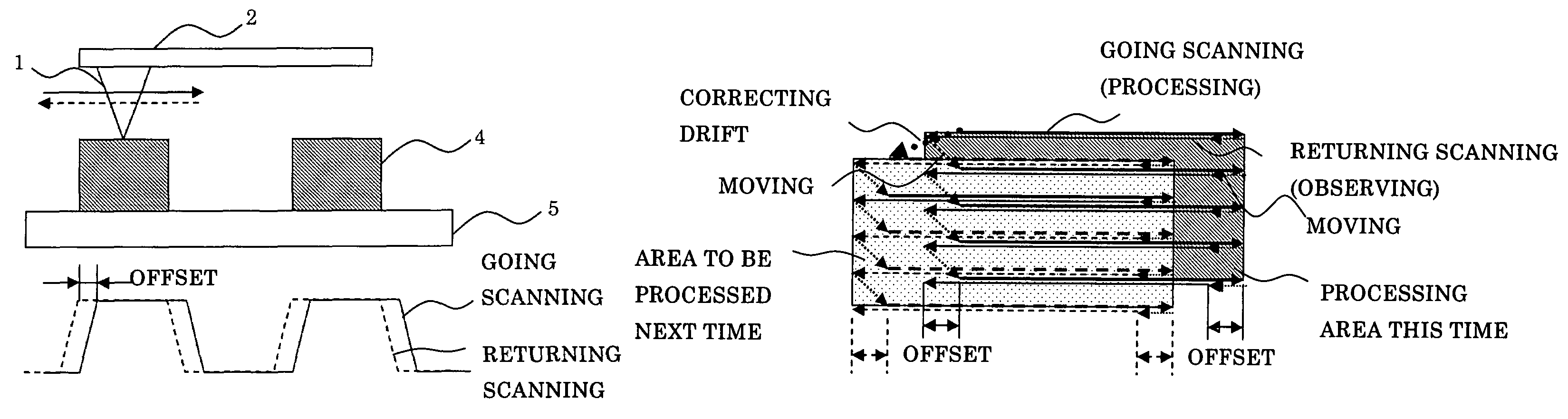
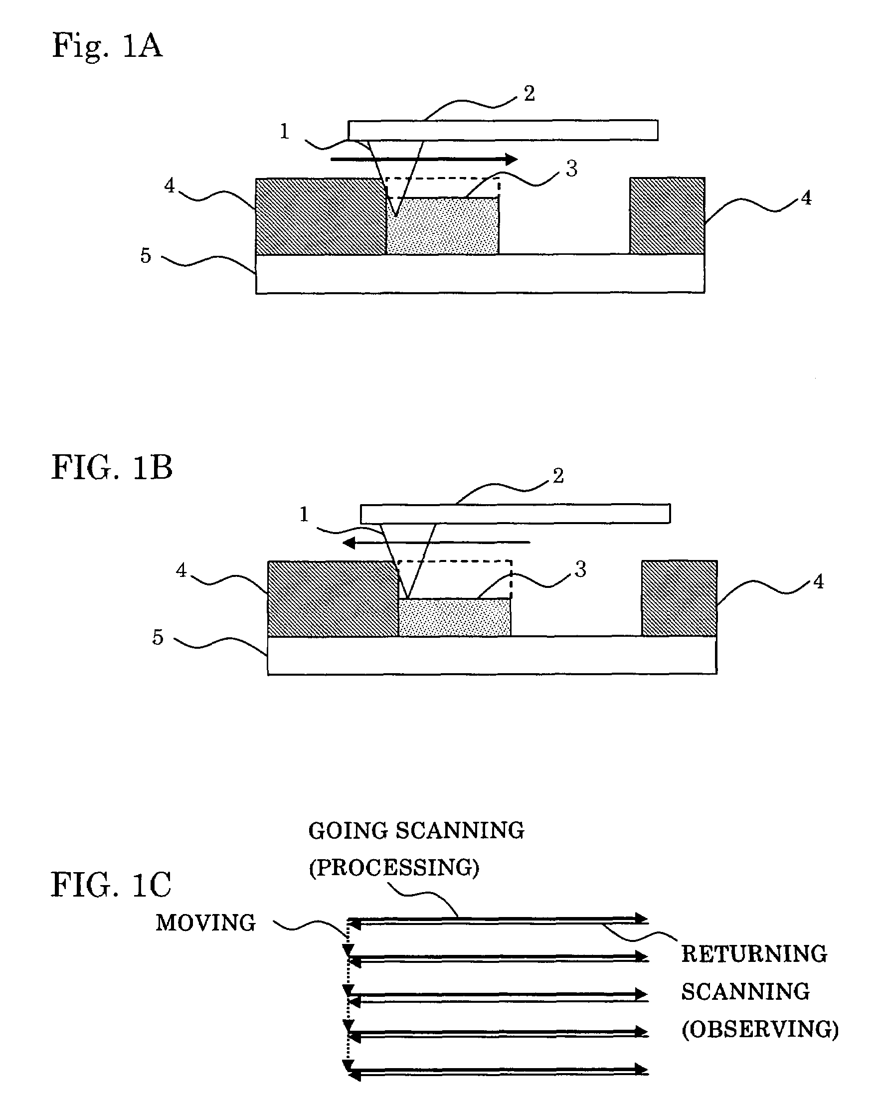
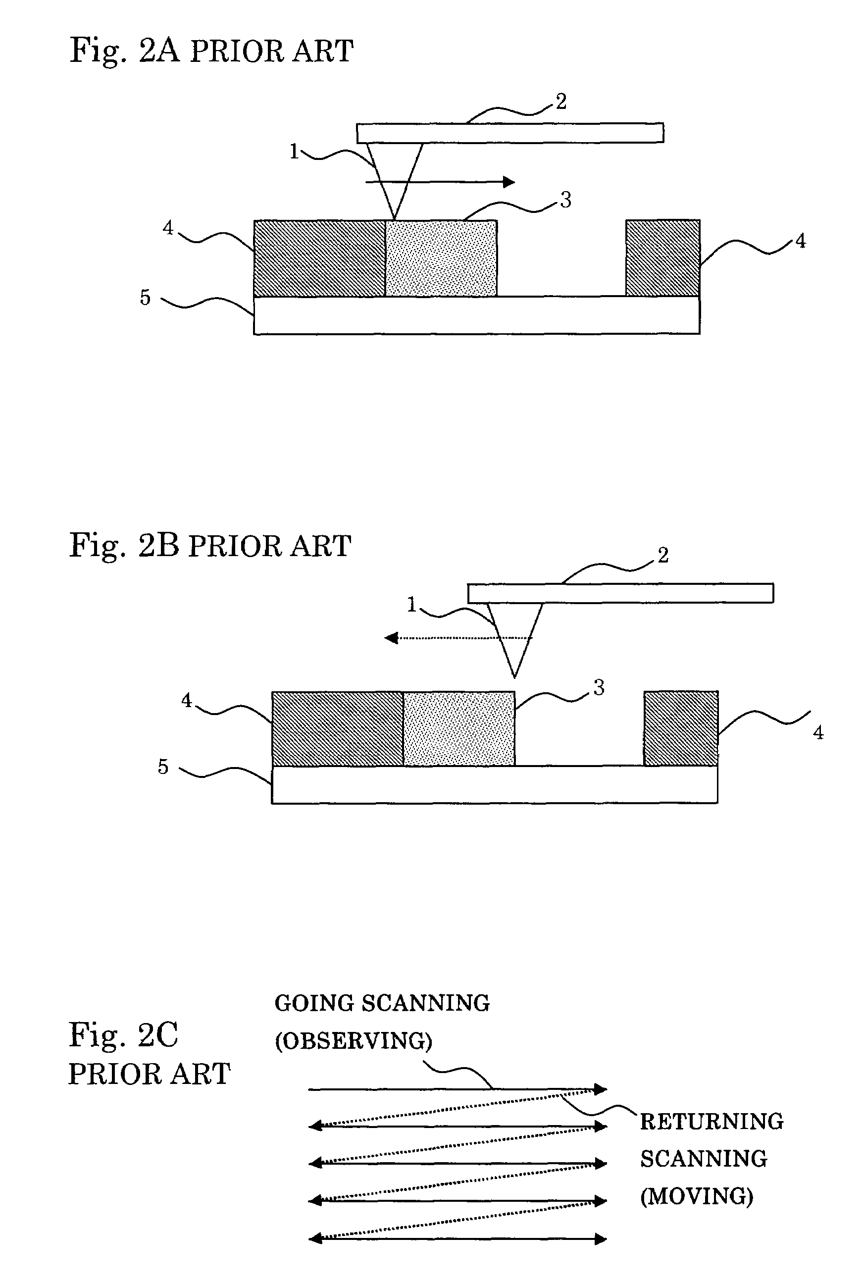
[0025]A photomask having an opaque defect found by a defect inspection device is introduced into an atomic force microscope defect correcting device, and a high accuracy XY stage is moved so as to position the opaque defect portion at the center of a view. When an opaque defect 3 is extracted in the atomic force microscope defect correcting device, the conventional method is used. That is, in FIGS. 2A-2C, in the conventional scanning method (FIG. 2C) where the going scanning is for observing (FIG. 2A) and the returning scanning is performed while pulling up a probe to the height not to contact to a pattern and moving it to the next start point (FIG. 2B), an area including the opaque defect 3 is imaged having a contact mode or intermittent contact mode of the atomic force microscope so as to be compared with a normal pattern 4 by pattern matching or the like, and thus the opaqu...


PUM

PropertyMeasurementUnit
heightaaaaaaaaaa
atomic force microscopeaaaaaaaaaa
areaaaaaaaaaaa

Abstract

An opaque defect is processed by scanning with a high load or height fixed mode using a probe harder than a pattern material of a photomask at the time of going scanning, and is observed by scanning with a low load or intermittent contact mode at the time of returning scanning so as to detect an ending point of the opaque defect by the height information. When there is a portion reaching to a glass substrate as an ending point, this portion is not scanned by the high load or height fixed mode in the next processing, and only a portion not reaching to the ending point is scanned by the high load or height fixed mode.

Description

[0001]This application claims priority under 35 U.S.C. §119 to Japanese Patent Application No. JP2006-124678 filed Apr. 28, 2006, the entire content of which is hereby incorporated by reference.BACKGROUND OF THE INVENTION[0002]The present invention relates to an ending point detecting method and a drift correcting method for correcting an opaque defect of a photomask using an atomic force microscope technique.[0003]A fine processing technique in a nanometer order has been required in order to advance and make high integration of functions, and a processing technique such as a partial anodizing and oxidizing and a fine scratch processing using a scanning probe microscope (SPM) has been famously researched and developed. Recently, a practical processing device has been required to form an accurate shape and have high accurate processing, in addition to pursuit the fine processing property.[0004]An example of a recent device based on an atomic force microscope (AFM), which is required ...

Claims


Application Information

Patent Timeline
Patent Type & Authority Patents(United States)
IPC IPC(8): G01B5/28G03F1/00G03F1/72H01L21/027
CPCB82Y35/00G03F1/72G01Q30/06B82Y10/00G01Q10/06G01Q80/00
Inventor DOI, TOSHIOWATANABE, KAZUTOSHITAKAOKA, OSAMUUEMOTO, ATSUSHI
Owner HITACHI HIGH TECH SCI CORP
Why Eureka
Try Eureka