
Interface circuit system and method for performing power saving operations during a command-related latency

a power saving operation and interface circuit technology, applied in the field of memory, can solve the problems of limited power that may be dispersed per unit volume in the space available to the memory circuit, limited in terms of power, and limited in terms of ability

Active Publication Date: 2009-08-25
GOOGLE LLC
View PDF528 Cites 135 Cited by
  • Summary
  • Abstract
  • Description
  • Claims
  • Application Information

AI Technical Summary

Benefits of technology

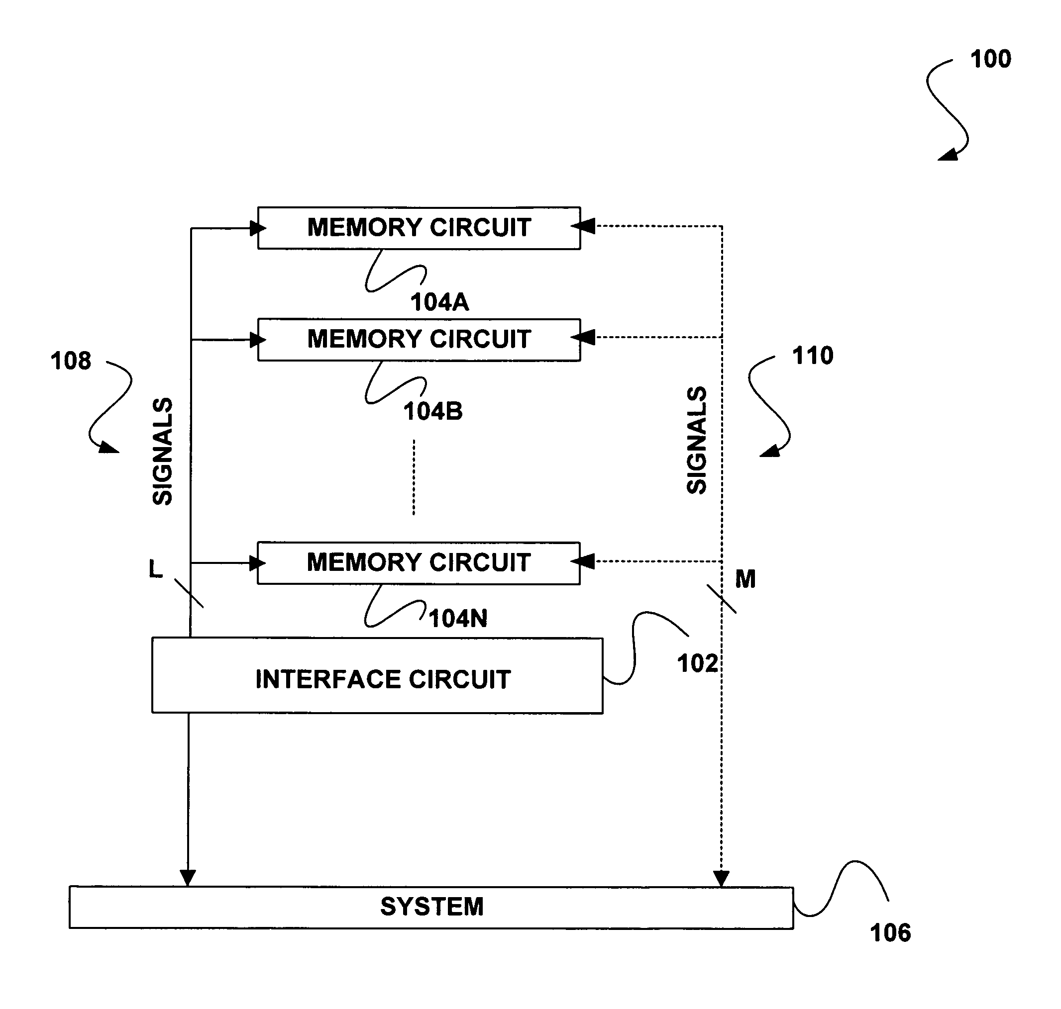
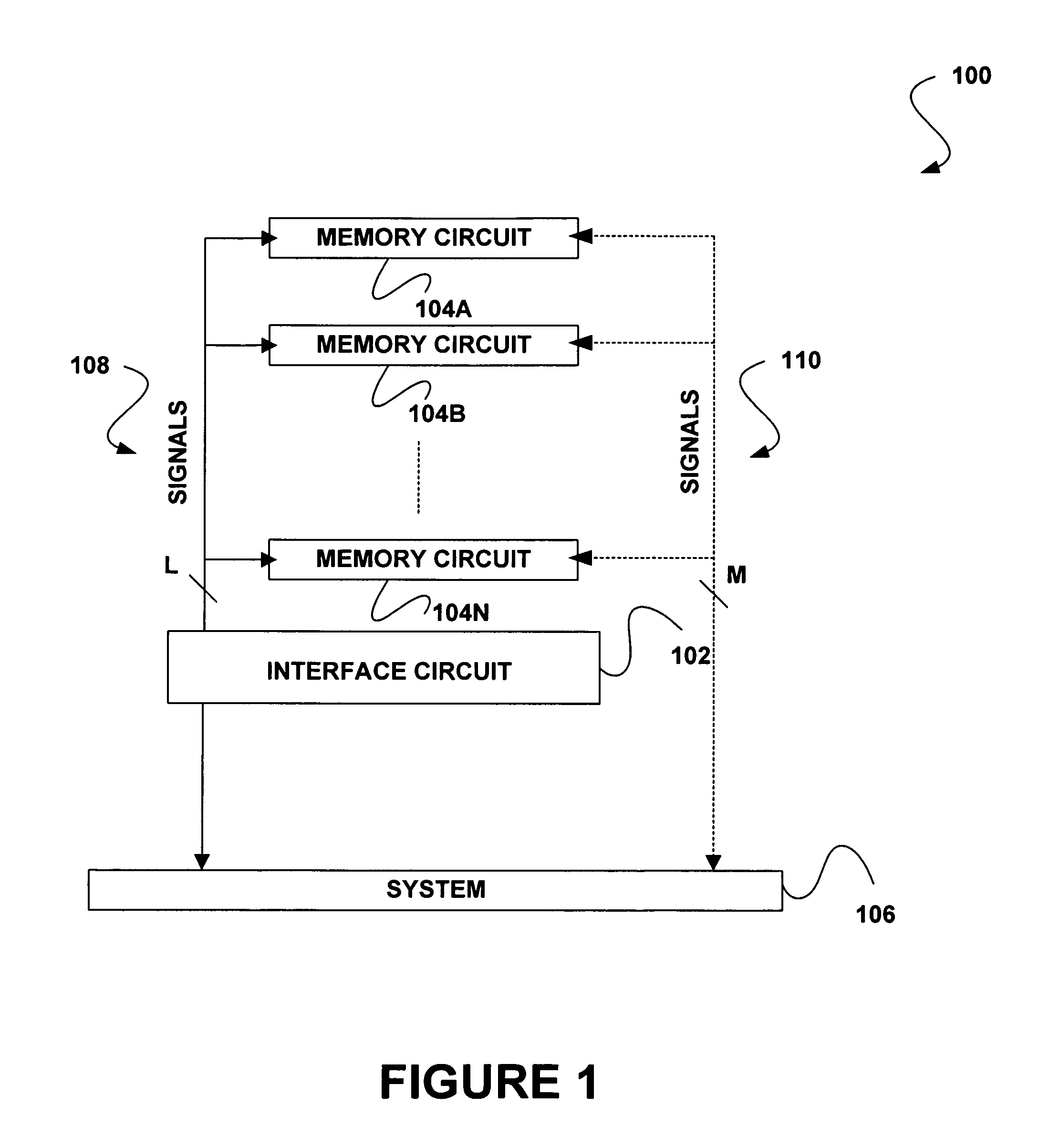
[0005]A memory circuit power management system and method are provided. In use, an interface circuit is in communication with a plurality of memory circuits and a system. The interface circuit is operable to interface the memory circuits and the system ...

Problems solved by technology

However, there is also a limit to the power that may be dissipated per unit volume in the space available to the memory circuits.
As a result, large capacity memory modules may be limited in terms of power that the memory modules may dissipate, and / or limited in terms of the ability of power supply systems to deliver sufficient power to such memory modules.

Method used


Image

  • Interface circuit system and method for performing power saving operations during a command-related latency
  • Interface circuit system and method for performing power saving operations during a command-related latency
  • Interface circuit system and method for performing power saving operations during a command-related latency

Examples


first embodiment

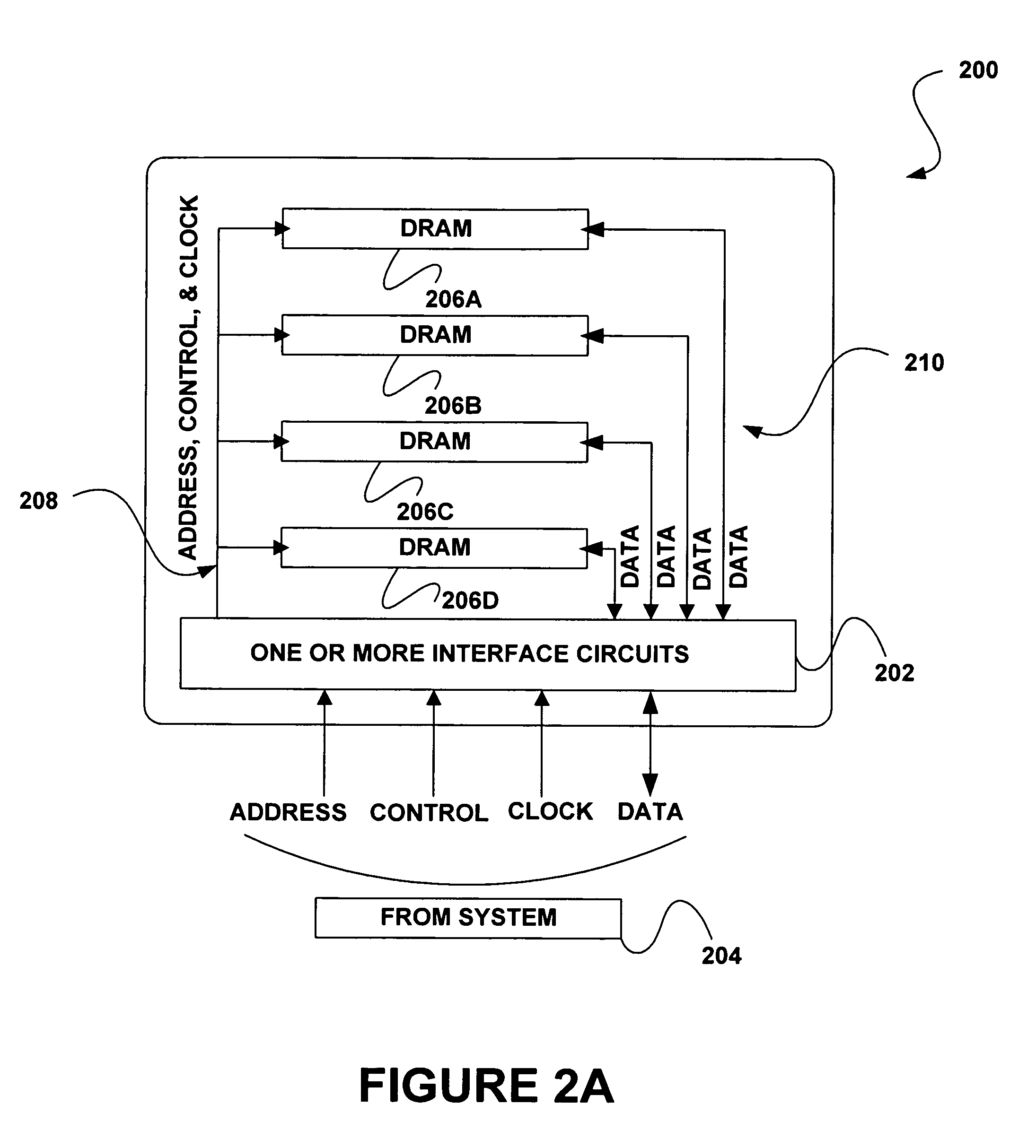
[0124]In a first embodiment, a row activate time based power management scheme may be used for one-circuit-to-many-bank configurations. In this embodiment, the power down entry latency of a physical DRAM circuit may be hidden behind the command operation period of an activate command directed to a different physical DRAM circuit. Additionally, the power down exit latency of a physical DRAM circuit may be hidden behind the command operation period of an activate command directed to itself. The activate command operation periods that are used to hide power down entry and exit latencies may be tRRD and tRCD respectively.

second embodiment

[0125]In a second embodiment, a row activate time based power management scheme may be used for many-circuit-to-one-bank and one-circuit-to-one-bank configurations. In this embodiment, the power down entry and exit latencies of a physical DRAM circuit may be hidden behind the command operation period of an activate command directed to itself. In this embodiment, the command operation period of an activate command may be tRCD.

[0126]In the first embodiment, a row activate time based power management scheme may place a first DRAM circuit that has no open banks into a power down mode when an activate command is issued to a second DRAM circuit if the first and second DRAM circuits are part of a plurality of physical DRAM circuits that appear as a single virtual DRAM circuit to the memory controller. This power management scheme may allow each DRAM circuit to enter power down mode when not in use. This embodiment may be used in one-circuit-to-many-bank configurations of DRAM circuits. Whi...


PUM


Abstract

A memory circuit power management system and method are provided. In use, an interface circuit is in communication with a plurality of memory circuits and a system. The interface circuit is operable to interface the memory circuits and the system for performing a power management operation in association with at least a portion of the memory circuits. Such power management operation is performed during a latency associated with one or more commands directed to at least a portion of the memory circuits.

Description

RELATED APPLICATION(S)[0001]The present application is a continuation of an application filed Sep. 20, 2006 under application Ser. No. 11 / 524,811, which is a continuation-in-part of an application filed Jul. 31, 2006 under application Ser. No. 11 / 461,439, which are each incorporated herein by reference for all purposes. However, insofar as any definitions, information used for claim interpretation, etc. from the above parent application conflict with that set forth herein, such definitions, information, etc. in the present application should apply.FIELD OF THE INVENTION[0002]The present invention relates to memory, and more particularly to power management in multiple memory circuit systems.BACKGROUND[0003]The memory capacity requirements of various systems are increasing rapidly. However, other industry trends such as higher memory bus speeds and small form factor machines, etc. are reducing the number of memory module slots in such systems. Thus, a need exists in the industry for ...

Claims


Application Information

Patent Timeline
IPC IPC(8): G06F1/32
CPCG11C5/04G11C5/14G11C5/145G11C11/4074G11C7/22G11C2207/2272G11C11/4076G11C11/4093G11C2207/2227
Inventor RAJAN, SURESH NATARAJANSCHAKEL, KEITH R.SMITH, MICHAEL JOHN SEBASTIANWANG, DAVID T.WEBER, FREDERICK DANIEL
Owner GOOGLE LLC
Learn More