Gate Level Reconfigurable Magnetic Logic

a magnetic logic and gate technology, applied in the field of reprogrammable logic, can solve the problems of affecting the operation of the gate, and consuming a large amount of power, and achieve the effects of reducing the write current, and increasing the current density

Active Publication Date: 2010-02-18
QUALCOMM INC
View PDF9 Cites 126 Cited by
  • Summary
  • Abstract
  • Description
  • Claims
  • Application Information

AI Technical Summary

Benefits of technology

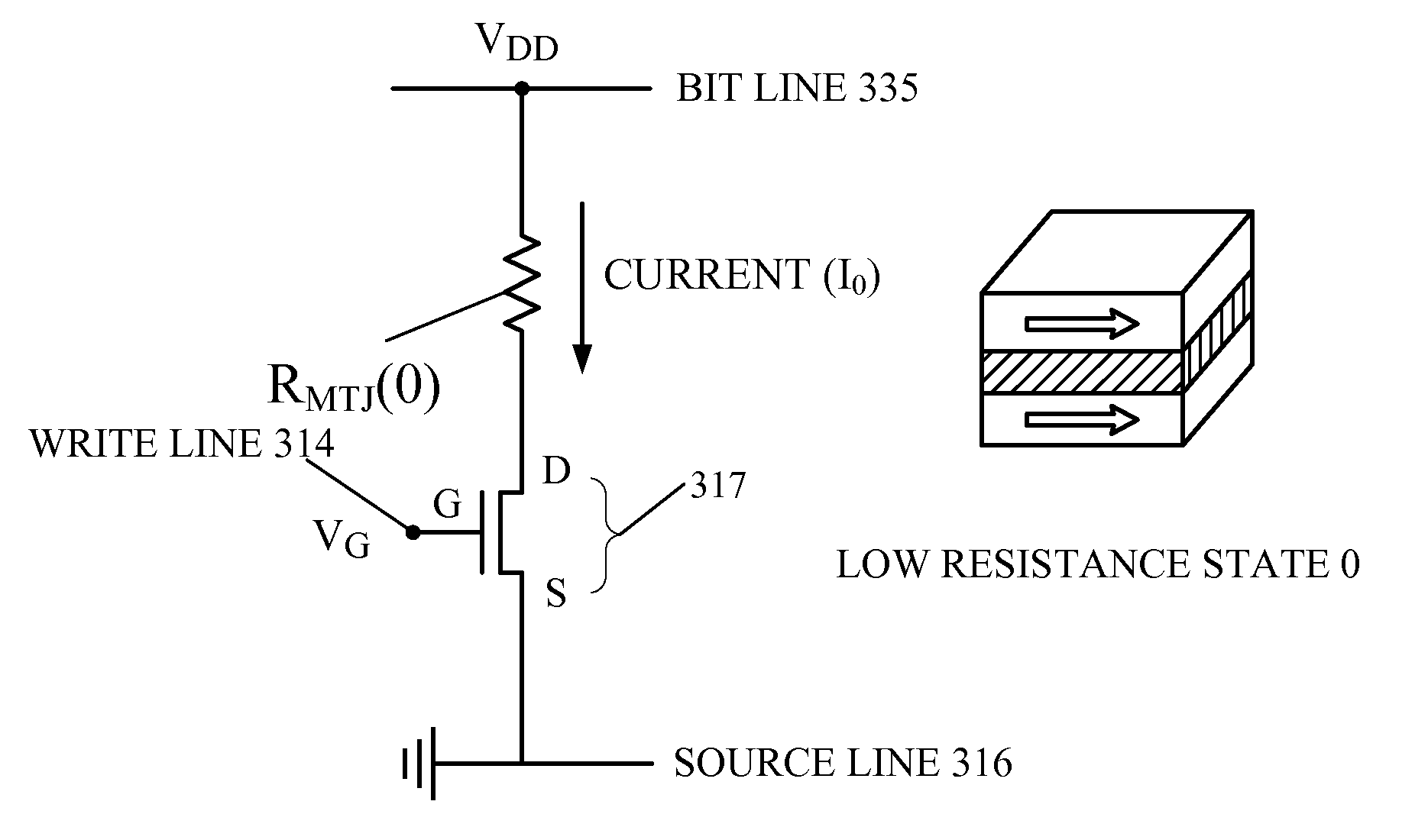
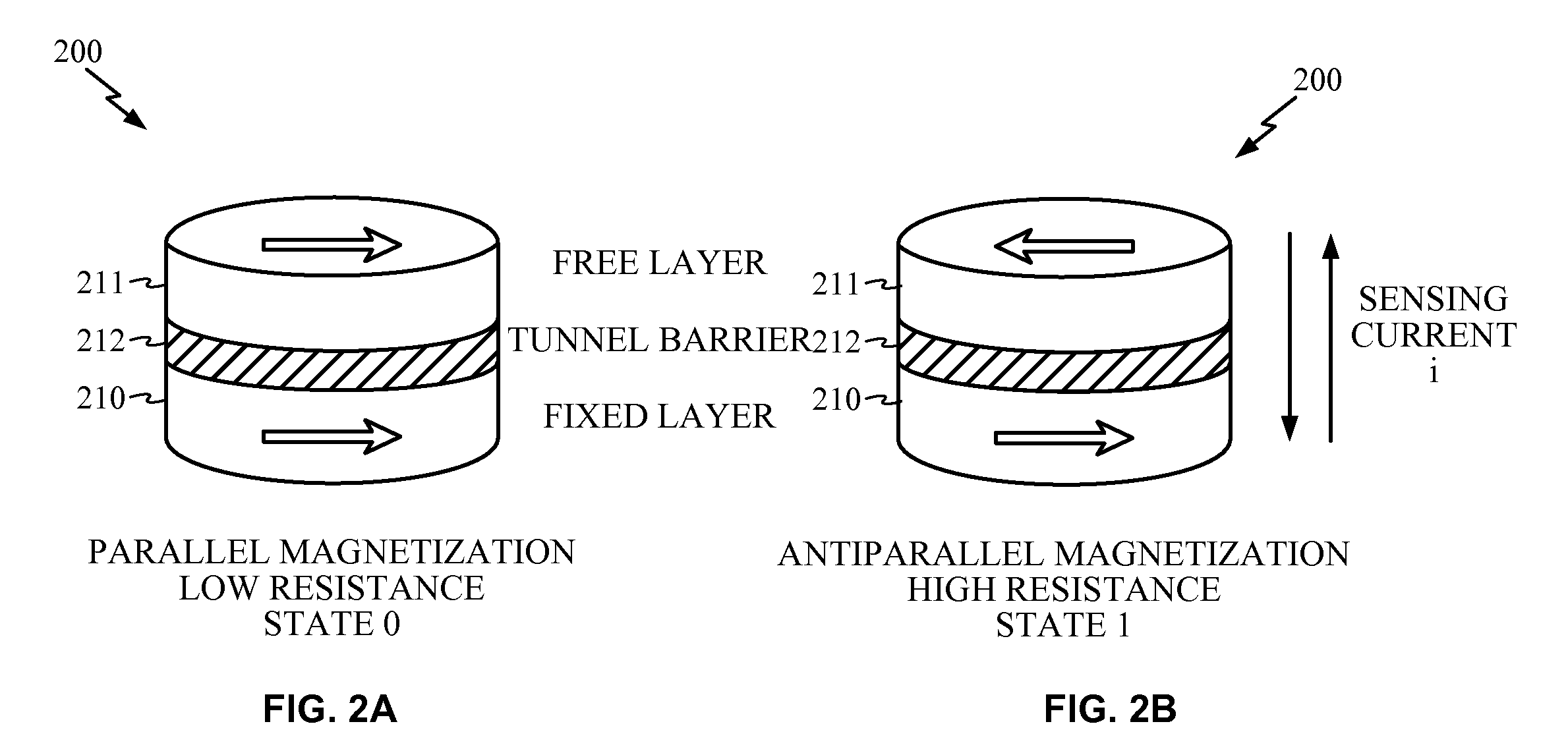
[0008]An STT MRAM element is a junction comprising a sandwich of a magnetic film, oxide film, and magnetic film, in an elliptically shaped structure, similar to conventional MRAM, but may be scaled to much smaller dimension. Like conventional MRAM, STT MRAM has a fixed layer and a free (write-programmable) layer of magnetic film. The free layer is programmed by means of spin torque transfer of the electron spin polari...

Problems solved by technology

This is particularly true of PLAs that are embedded in more complex and numerous integrated circuits such as microprocessors.
FPGAs are usually slower and may draw more power than their application-specific integrated circuit (ASIC) counterparts.
With FPGA, there is a considerable ...

Method used


Image

  • Gate Level Reconfigurable Magnetic Logic
  • Gate Level Reconfigurable Magnetic Logic
  • Gate Level Reconfigurable Magnetic Logic

Examples


example 1

[0042]Assume the MTJ junctions J1-J4 are set to the states [1,0,1,0]. Therefore, the corresponding resistances are RJ-1(1)=5R0, RJ-2(0)=R0, RJ-3(1)=5R0, and RJ-4(0)=R0. For all four possible combinations of A,B and the resulting four input voltages [A, _A, B, _B] of magnitude VDD the measured voltage VT are shown in Table I.

TABLE 1Transistor voltage VT for junction states [1, 0, 1, 0] versus inputs A, BAA—BB—VT / VDD10100.1810010.4201100.4201010.67

[0043]FIG. 5A is a representative plot of voltage output VT(A,B) for the possible combinations of inputs shown in Table 1, given that the state settings for the four STT MTJ junctions J-1 to J-4 are [1,0,1,0]. The output voltage may be indexed relative to the input states A,B, i.e., as VT(A,B). Inverter 420 receives the voltage VT(A,B) from summing line 420. Inverter 430 may be set to trigger an output if VT(A,B) exceeds the a threshold voltage. Inverter 430 then may amplify the input to output a logical 1 or 0 level (e.g., VDD or 0) dependi...

example 2

[0046]Assume the MTJ junctions J-1 to J-4 are set to the states [0,1,0,1]. Therefore, the corresponding resistances are RJ-1(0)=R0, RJ-2(1)=5R0, RJ-3(0)=R0, and RJ-4(1)=5R0. Using the same analysis as above, FIG. 5B is a representative plot of voltage output VT(A,B) for the possible combinations of inputs, given that the state settings for the four STT MTJ junctions J-1 to J-4 are [0,1,0,1]. Note that VT(1,1) is the highest output, as compared to the first example, where VT(0,0) was highest. If inverter 430 is set to trigger between VT(1,1) and VT(1,0) and output VDD or 0 accordingly, the truth table in Table 4 results. It can be seen that F is identical to a logical AND, and F_ is identical to a logical NAND.

TABLE 4Truth Table for junction states [0, 1, 0, 1] versus inputs A, B,Threshold voltage set between VT(1, 1) and VT(1, 0)ABFF—1110100101010001ANDNAND

[0047]Similarly, if inverter 430 is set to trigger based on a threshold voltage between VT(1,0) and VT(0,0), the truth table in ...


PUM


Abstract

A re-programmable gate logic includes a plurality of non-volatile re-configurable resistance state-based memory circuits in parallel, wherein the circuits are re-configurable to implement or change a selected gate logic, and the plurality of non-volatile re-configurable resistance state-based memory circuits are each adapted to receive a logical input signal. An evaluation switch in series with the plurality of parallel non-volatile re-configurable resistance state-based memory circuits is configured to provide an output signal based on the programmed states of the memory circuits. A sensor is configured to receive the output signal and provide a logical output signal on the basis of the output signal and a reference signal provided to the sensor. The reconfigurable logic may be implemented based on using spin torque transfer (STT) magnetic tunnel junction (MTJ) magnetoresistance random access memory (MRAM) as the re-programmable memory elements. The logic configuration is retained without power.

Description

TECHNICAL FIELD[0001]This disclosure relates to programmable logic, and more specifically to reprogrammable logic using spin transfer torque magnetoresistance random access memory (STT MRAM).BACKGROUND[0002]A programmable logic array (PLA) is a programmable device used to implement combinational logic circuits. The PLA has a set of programmable AND planes, which link to a set of programmable OR planes, which can then be conditionally complemented to produce an output. This layout allows for a large number of logic functions to be synthesized, including XOR or more complex combinational functions. Many PLAs are mask-programmed during manufacture in the same manner as a ROM. This is particularly true of PLAs that are embedded in more complex and numerous integrated circuits such as microprocessors. PLAs that can be programmed after manufacture are called FPLAs (field-programmable PLAs) or FPGAs (field-programmable gate arrays). FPGA interconnects can be programmed (i.e., “burned in”) ...

Claims


Application Information

Patent Timeline
IPC IPC(8): H03K19/173
CPCG11C11/16H03K19/1776H03K19/18G11C11/15H03K19/173
Inventor CHUA-EOAN, LEW G.ZHU, XIAOCHUNZHU, ZHI
Owner QUALCOMM INC
Why Eureka
Try Eureka