

Device with embedded high-bandwidth, high-capacity memory using wafer bonding
a high-capacity memory and high-bandwidth technology, applied in the field of high-performance computing, can solve the problems of dram arrays with a much lower density per unit area of silicon substrates, large power consumption, and substantial delay
- Summary
- Abstract
- Description
- Claims
- Application Information
AI Technical Summary
Benefits of technology
Problems solved by technology
Method used
Image

Examples
Embodiment Construction
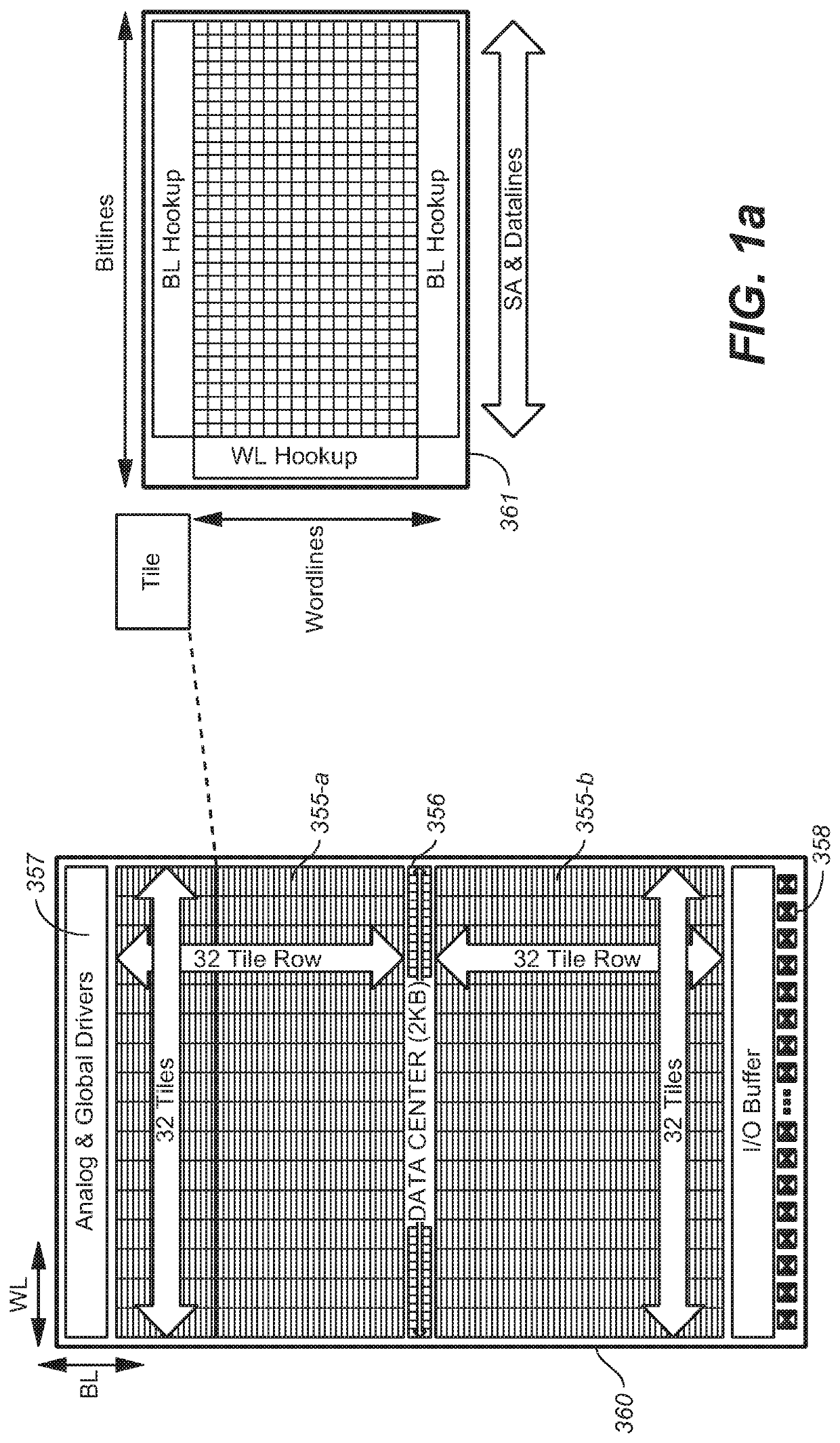
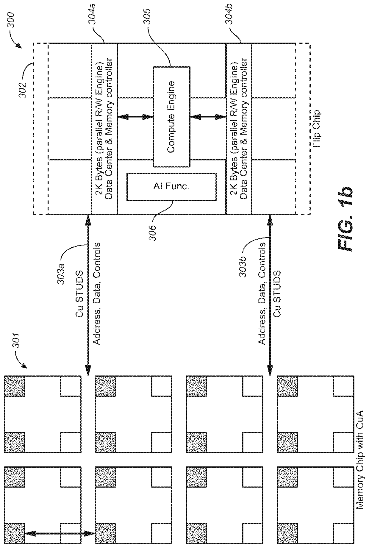
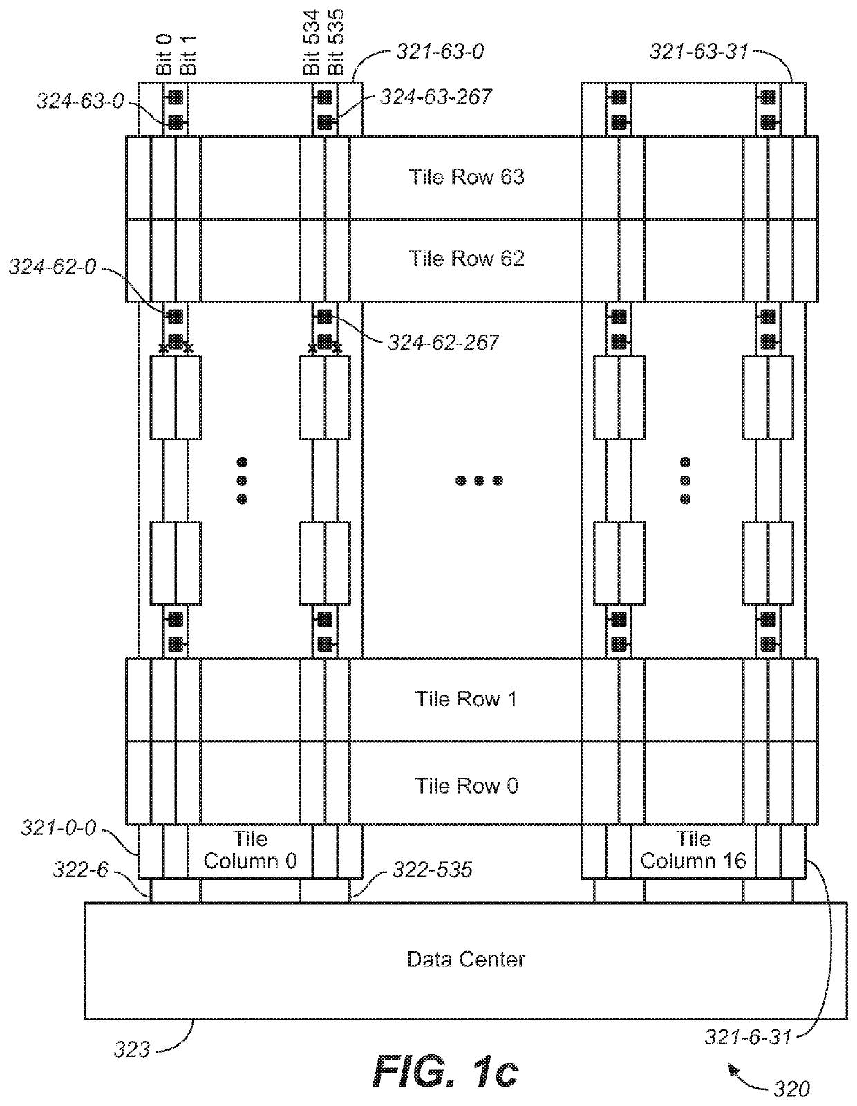
[0050]A powerful electronic device of the present invention is formed by combining a memory circuit fabricated on one semiconductor die (e.g., a 3-D NOR memory chip) with a complex logic circuit (e.g., a memory controller, one or more multi-core processor, a field programmable logic circuit, or a neural network) formed on a second semiconductor die using a wafer-bonding or die-bonding technique. Preferably, the memory circuit comprises one or more regular arrays of addressable modular structures or building blocks of memory cells (“tiles”) placed in a regular manner The modularity allows the memory circuit to be segmented into independently addressable memory segments. For example, a memory segment of a desired size (e.g., a row of 32 tiles) may be achieved by configuring a group of tiles to form the memory segment, as desired.
[0051]The present invention is particularly advantageous when the memory circuit is one of the high-capacity and fast-access memory circuits disclosed in the ...
PUM
 Abstract
Description
Claims
Application Information