Chip package and coreless package substrate thereof

a coreless package and chip technology, applied in the direction of semiconductor devices, semiconductor/solid-state device details, electrical apparatus, etc., can solve the problems of hard reduction of i>f /i>, the pitch of the plating through holes (pths) is not easy to be smooth, etc., to promote the co-planarity of the coreless package substrate, reduce the residual stress, and increase the strength

Active Publication Date: 2009-09-08
VIA TECH INC
View PDF4 Cites 14 Cited by
  • Summary
  • Abstract
  • Description
  • Claims
  • Application Information

AI Technical Summary

Benefits of technology

[0011]According to an aspect of the present invention, because the ceramic stiffener in the coreless package substrate of the present invention has substantially higher strength compared to the conventional metal stiffener, during the process of fabricating the coreless package substrate the ceramic stiffener is unlikely to warp and also capable of reducing the residual stress in the coreless package substrate, and thereby promote the co-planarity of the coreless package substrate. Moreover, since the coreless package substrate of the present invention does not have any plating through hole (PTH), the wiring density of the coreless package substrate is increased. In addition, since the ceramic stiffener in the coreless package substrate of the present invention has a second opening or a second inner circuit, electronic components can be disposed in the second opening or on the ceramic stiffener for further increasing the disposition area of the electronic components.

Problems solved by technology

In the conventional flip chip package however, the pitch of the plating through holes (PTHs) 112f is hard to be reduced, which becomes a major bottleneck while the layout density of the substrate 110 is increased.

Method used


Image

  • Chip package and coreless package substrate thereof
  • Chip package and coreless package substrate thereof
  • Chip package and coreless package substrate thereof

Examples


Embodiment Construction

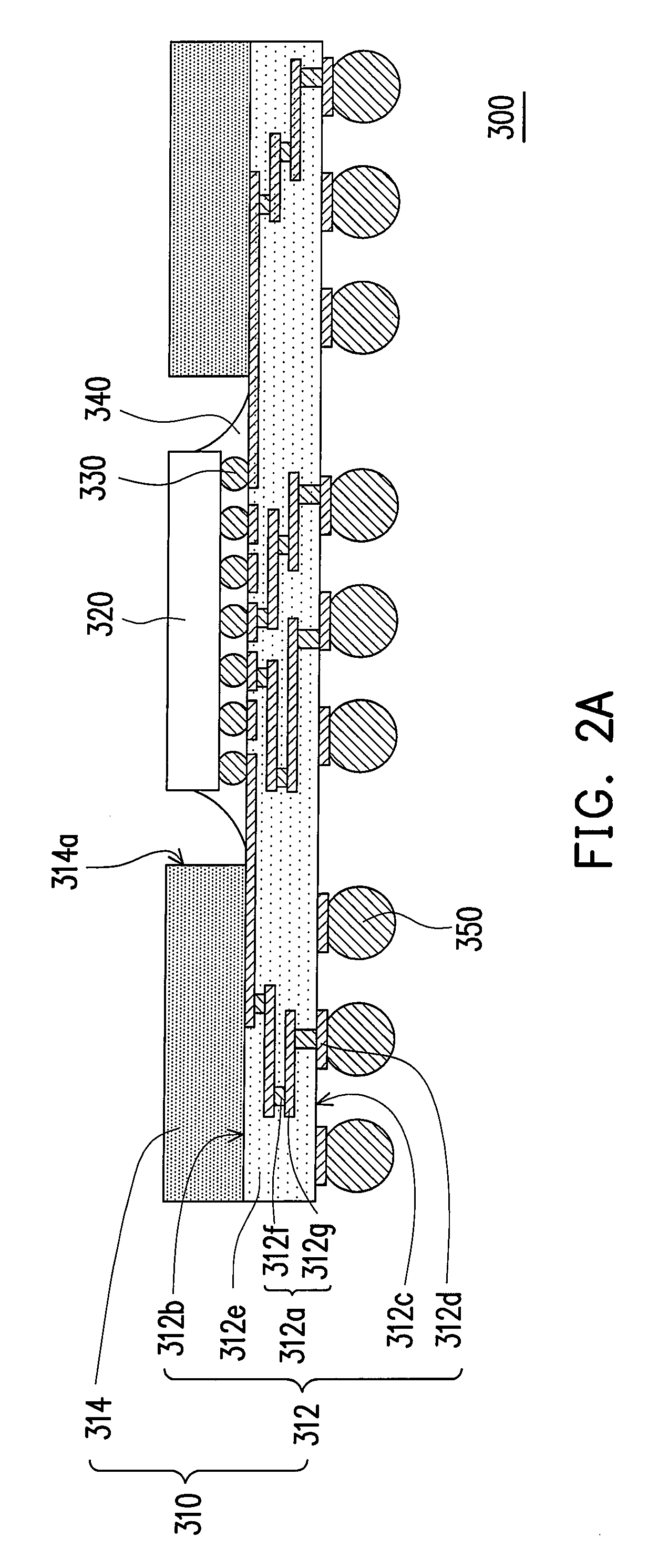
[0019]FIG. 2A is a schematic cross-sectional view of a chip package according to the first embodiment of the present invention, while FIG. 2B is a schematic top view of the chip package in FIG. 2A. Referring to FIGS. 2A and 2B, a chip package 300 of the first embodiment includes a coreless package substrate 310 and a chip 320. The coreless package substrate 310 includes an interconnection structure 312 and a ceramic stiffener 314. The interconnection structure 312 has a first inner circuit 312a, a carrying surface 312b and a corresponding contact surface 312c. The first inner circuit 312a has a plurality of contact pads 312d disposed on the contact surface 312c. The ceramic stiffener 314 is disposed on the carrying surface 312b and has a first opening 314a. Besides, the chip 320 is disposed on the carrying surface 312b and within the first opening 314a and is electrically connected to at least one of the contact pads 312d. In the first embodiment, the first opening 314a herein has a...


PUM


Abstract

A chip package includes a coreless package substrate and a chip. The coreless package substrate includes an interconnection structure and a ceramic stiffener. The interconnection structure has a first inner circuit, a carrying surface and a corresponding contact surface. The first inner circuit has multiple contact pads disposed on the contact surface. The ceramic stiffener is disposed on the carrying surface and has a first opening. In addition, the chip is disposed on the carrying surface and within the first opening and electrically connected to at least one of the contact pads.

Description

CROSS-REFERENCE TO RELATED APPLICATION[0001]This application claims the priority benefit of Taiwan application serial no. 94144010, filed on Dec. 13, 2005. All disclosure of the Taiwan application is incorporated herein by reference.BACKGROUND OF THE INVENTION[0002]1. Field of the Invention[0003]The present invention relates to a semiconductor device and a carrier thereof, and more particularly to a chip package and a coreless package substrate thereof.[0004]2. Description of Related Art[0005]In the semiconductor industry, an integrated circuit (IC) is fabricated through three phases including an IC design, an IC process and an IC packaging. In the IC process, a chip is fabricated by forming ICs on the wafer and then dicing the wafer. A wafer has an active surface, which generally refers to a surface having active devices thereon. After forming the ICs on the wafer, a plurality of bonding pads are disposed on the active surface of the chip and the chip finally made by dicing the waf...

Claims


Application Information

Patent Timeline
Patent Type & Authority Patents(United States)
IPC IPC(8): H01L23/00H01L23/58
CPCH01L23/49833H01L24/81H01L2224/2919H01L2224/73204H01L2224/32225H01L2224/16225H01L2924/19105H01L2924/15311H01L2924/15174H01L2924/1517H01L2924/15153H01L2924/01078H01L24/83H01L2224/16H01L2224/8121H01L2224/81815H01L2224/83851H01L2924/00H01L2924/00014H01L2924/14
Inventor CHANG, WEN-YUAN
Owner VIA TECH INC
Why Eureka
Try Eureka