Organic EL drive circuit and organic EL display device using the same organic EL drive circuit

a drive circuit and drive circuit technology, applied in static indicating devices, instruments, electroluminescent light sources, etc., can solve the problems of uneven luminance on the display screen of an organic el display device, high fabrication cost of the driver ic's, and large organic el panel size, so as to reduce the fabrication cost of the column driver ic's and reduce the uneven luminance

Active Publication Date: 2009-09-08
ROHM CO LTD
View PDF12 Cites 2 Cited by
  • Summary
  • Abstract
  • Description
  • Claims
  • Application Information

AI Technical Summary

Benefits of technology

[0017]An object of the present invention is to provide an organic EL drive circuit, which is capable of reducing luminance unevenness on a display screen of an organic EL display device due to difference in characteristics between column driver IC's for driving an organic EL panel and of reducing the fabrication cost of column driver IC's.
[0023]As a result, unevenness of drive currents outputted from the output terminals of the respective IC's is reduced, so that unevenness of luminance on the display screen of the organic EL display device due to variation in characteristics between the column driver IC's, which drive the organic EL panel, is reduced.
[0024]Particularly, by arranging a plurality of second output side transistors on an upstream side of the first output side transistors with respect to the input side transistor of the current mirror circuit, the respective second output side transistors can provide reference currents to a plurality of slave IC's. As a result, the master IC can drive the plurality of the slave IC's, so that unevenness of currents outputted from the respective output terminals of the master and slave IC's can be restricted.
[0025]By providing two input side transistors in the current mirror circuit on both sides of the first and second output side transistors and driving the first and second output side transistors from the both sides of the output side transistors arrangement, it is possible to reduce difference between the last column line of a certain drive IC as a master drive IC and the first column line of a next drive IC as a slave driver IC, to thereby reduce luminance unevenness on the display screen.
[0026]As a result, according to the present invention, unevenness of luminance on the display screen of the organic EL display device of such as a portable telephone set, which is due to difference in characteristics between the column driver IC's for driving the organic EL panel can be reduced even when the number of terminal pins is increased. Further, since any one of the column driver IC's can be used as either the master IC or the slave IC, it is possible to reduce the fabrication cost of the column driver IC's.

Problems solved by technology

Therefore, there is a problem that unevenness of luminance appears on a display screen of an organic EL display device, due to difference in characteristics between column driver IC's and, particularly, due to variation of drive currents of the column driver IC's.
Therefore, the fabrication cost of the driver IC's becomes high.
On the other hand, the size of the organic EL panel tends to become larger.
Moreover, the increase of the number of terminal pins makes unevenness of drive currents of terminal pins considerable.
As to the drive current control utilizing the paired resistors disclosed in JP2003-288045A, since unevenness of resistance values of the paired resistors influences the drive currents, the use of paired resistors can not respond to the present request of further reduction of luminance unevenness.

Method used


Image

  • Organic EL drive circuit and organic EL display device using the same organic EL drive circuit
  • Organic EL drive circuit and organic EL display device using the same organic EL drive circuit
  • Organic EL drive circuit and organic EL display device using the same organic EL drive circuit

Examples


Embodiment Construction

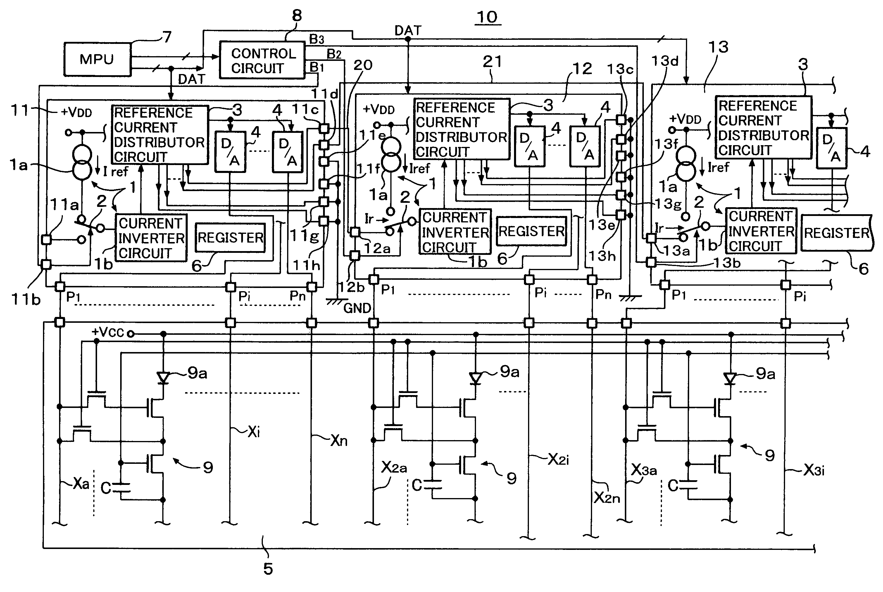
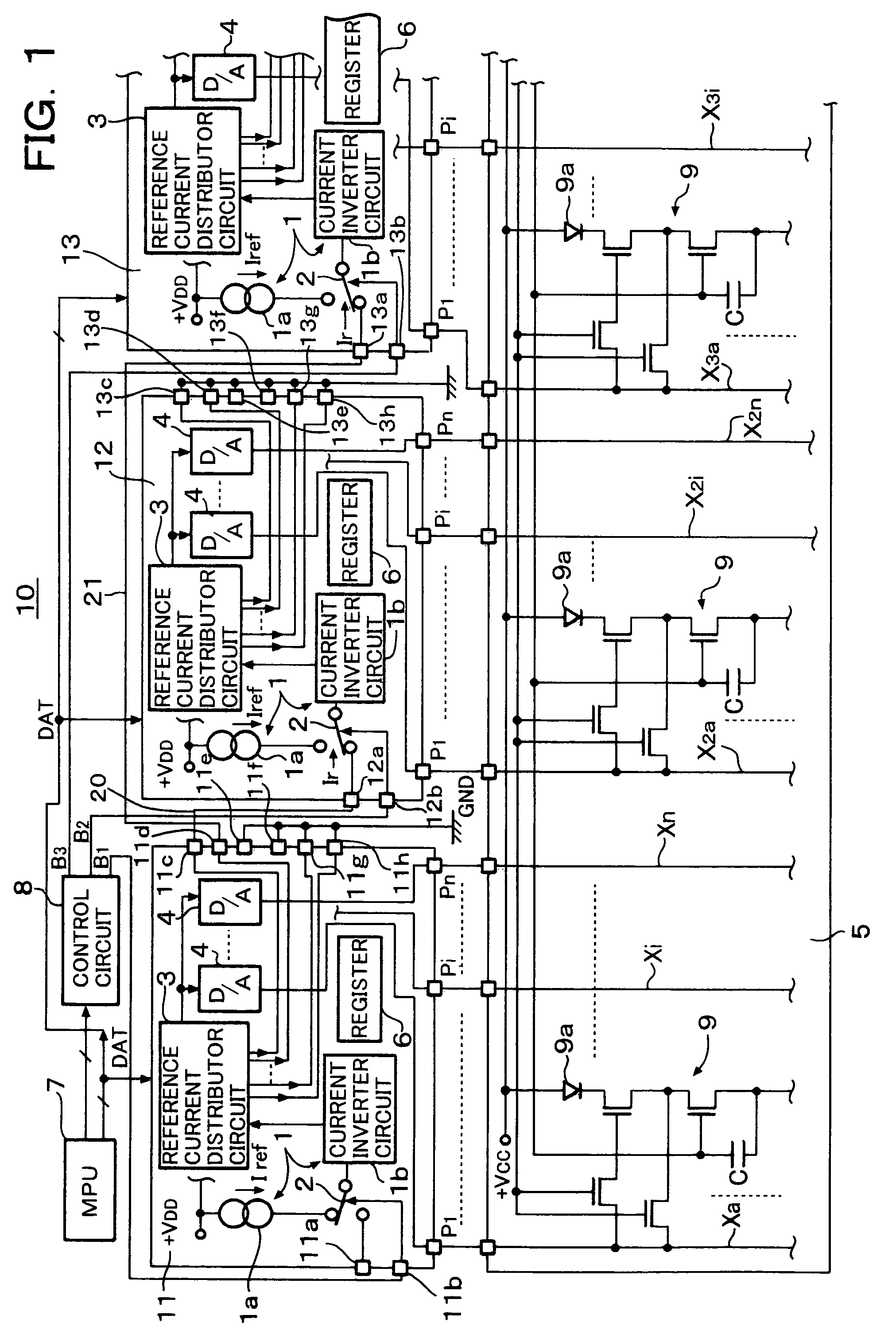
[0031]In FIG. 1, a reference numeral 10 depicts an organic EL display device of active matrix type and reference numerals 11, 12 and 13 depict column driver IC's of an organic EL drive circuit of the organic EL display device.

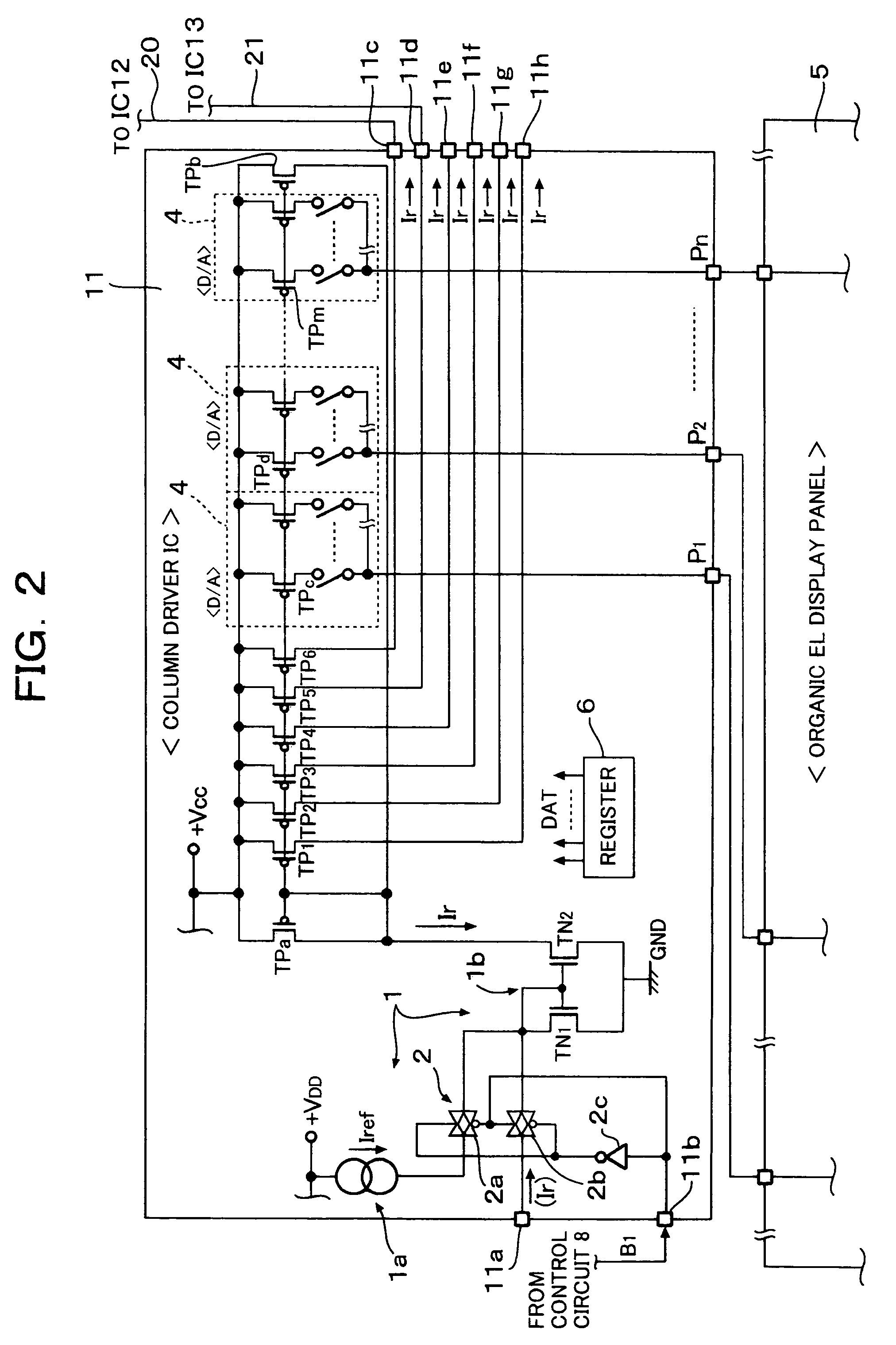
[0032]The column driver IC's 11 to 13 have identical constructions and each of them, for example, the column driver IC 11, is constructed with a reference current generator circuit 1, a reference current selector circuit 2, a reference current distributor circuit 3 and D / A conversion blocks 4 provided for respective terminal pins of the organic EL panel as shown in detail in FIG. 2.

[0033]The D / A conversion blocks 4 of each of the column driver IC's 11, 12 and 13 are responsive to display data DAT from an MPU 7 through a register 6 to amplify a reference drive current generated by the reference current generator circuit 1 according to the display data and generate drive currents (discharge currents) correspondingly to display luminance every moment. The thus gen...


PUM


Abstract

A current inputted from a first input terminal and a reference current generated by an internal reference current generator circuit, which are in phase, are inputted to a reference current selector circuit by which either the inputted current or the reference current is selected. The selected current is temporarily phase-inverted by a current inverter circuit and drives a current mirror circuit of a current distributor circuit (or a reference current regulator circuit) for duplicating the reference current and distributing them. Currents, each of which is in phase with the reference current or the inputted current and has same current value as that of the reference current or the inputted current, can be generated in the output side transistors of the current mirror circuit. In order to realize this, a second output side transistor is provided in the current mirror circuit so that a current, which is in phase with the reference current and has substantially equal value to that of the selected current, is supplied from the output terminal to a next stage integrated circuit as an input reference current.

Description

BACKGROUND OF THE INVENTION[0001]1. Field of the Invention[0002]The present invention relates to an organic EL drive circuit and an organic EL display device using the same organic EL drive circuit and, in particular, to an organic EL drive circuit and an organic EL display device, which can reduce unevenness of luminance on a display screen of an organic EL panel of the organic EL display device used in a portable telephone set, etc., due to difference in characteristics between column driver IC's, can reduce manufacturing cost of the column driver IC's and, particularly, is suitable for high luminance color display.[0003]2. Description of the Related Art[0004]An organic EL display panel of an active or passive type organic EL display device for use in a portable telephone set including 396 (132×3) terminal pins (column pins) for column lines (anode side drive lines of organic EL elements or data lines) and 162 terminal pins for row lines has been proposed. These numbers of the ter...

Claims


Application Information

Patent Timeline
Patent Type & Authority Patents(United States)
IPC IPC(8): G09G3/30G09G3/20G09G3/32H01L51/50H05B33/14H05B44/00
CPCG09G3/325G09G3/3283G09G2320/0233G09G2310/027G09G2300/0842G09G3/30G09G3/20
Inventor FUJISAWA, MASANORIABE, SHINICHIYAGUMA, HIROSHI
Owner ROHM CO LTD
Why Eureka
Try Eureka