Liquid crystal device and electronic apparatus

a liquid crystal device and electronic equipment technology, applied in non-linear optics, instruments, optics, etc., can solve the problems of misalignment between transmisive display regions and reflective display regions, grainy, stain-like irregularities, etc., to eliminate the difference in retardation, high brightness, and high contrast

Inactive Publication Date: 2009-09-08
JAPAN DISPLAY WEST
View PDF26 Cites 11 Cited by
  • Summary
  • Abstract
  • Description
  • Claims
  • Application Information

AI Technical Summary

Benefits of technology

[0007]An advantage of the invention is that it provides a homeotropic liquid crystal device having a multigap structure with high brightness and high contrast.
[0008]A liquid crystal device according to an aspect of the invention includes a pair of substrates and a liquid crystal layer held between the substrates and containing a liquid crystal having negative dielectric anisotropy. The liquid crystal layer includes subpixels, each including a plurality of transmissive display regions and a reflective display region that are arranged in a predetermined direction. The transmissive display regions are disposed at the ends of each subpixel in the direction in which the transmissive and reflective display regions are arranged. The liquid crystal device further includes a thickness-adjusting layer disposed between at least one of the substrates and the liquid crystal layer so that the liquid crystal layer is thinner in the reflective display region than in the transmissive display regions.
[0009]This liquid crystal device can provide a wide-viewing-angle display because the liquid crystal having negative dielectric anisotropy is aligned perpendicularly to the surfaces of the substrates. In addition, the thickness-adjusting layer can eliminate the difference in retardation between the transmissive display regions and the reflective display region to achieve high contrast for both transmissive display and reflective display. Furthermore, the transmissive display regions are disposed at the ends of each subpixel in the direction in which the transmissive and reflective display regions are arranged. Thus, tapered steps formed on the thickness-adjusting layer between the transmissive and reflective display regions are not located at the boundaries between the subpixels adjacent in the direction in which the transmissive and reflective display regions are arranged. Liquid crystal molecules located at the tapered steps are inclined with respect to the direction normal to the substrates. Such liquid crystal molecules are largely tilted by the action of transverse electric fields occurring between the subpixels adjacent in the longitudinal direction thereof as compared to those aligned in the direction normal to the substrates. This results in larger light leakage. According to the aspect of the invention, by contrast, the liquid crystal molecules located at the tapered steps are less susceptible to the transverse electric fields because the tapered steps are separated from the areas where the transverse electric fields occur. The transverse electric fields act on liquid crystal molecules located in areas where the liquid crystal layer has a uniform thickness, although the molecules cause little light leakage in such areas. The liquid crystal device according to the aspect of the invention can thus effectively prevent light leakage at the boundaries between the subpixels to provide a high-contrast display.
[0010]According to the technical idea of separating the tapered steps from the boundaries between the subpixels, the thickness-adjusting layer can also be disposed across the boundaries between the subpixels adjacent in the longitudinal direction so that the reflective display regions are located at the ends of the subpixels in the longitudinal direction. If such a structure is applied to transflective liquid crystal devices, in which the area of transmissive display region is larger than that of reflective display region in each subpixel, the reflective display region is divided in two regions on both sides of the transmissive display region. Such divided reflective display regions have been found to have a low reflectance relative to the area thereof and thus decrease the substantial aperture ratio of the liquid crystal devices. According to the aspect of the invention, by contrast, each subpixel includes the divided transmissive display regions and the single reflective display region, which can have the reflectance corresponding to the area thereof. The structure according to the aspect of the invention is thus suitable for liquid crystal devices in which the total area of reflective display region is smaller than that of transmissive display region in each subpixel.
[0011]The liquid crystal device according to the aspect of the invention preferably further includes a pixel drive unit that drives the subpixels by applying signals of opposite polarities to the subpixels adjacent in the direction in which the transmissive and reflective display regions are arranged. For example, the liquid crystal device preferably drives the subpixels by line inversion driving or dot inversion driving. Such driving methods effectively prevent flicker and crosstalk to provide a high-quality display. In line inversion driving or dot inversion driving, transverse electric fields occur between the subpixels corresponding to the adjacent lines. According to the aspect of the invention, as described above, the tapered steps of the thickness-adjusting layer are separated from the areas where the transverse electric fields occur, where the thickness-adjusting layer has a uniform thickness. The liquid crystal device can therefore avoid misalignment due to the action of the transverse electric fields to provide a high-contrast display in line inversion driving and dot inversion driving.
[0012]The liquid crystal device according to the aspect of the invention preferably further includes island electrodes electrically connected to each other and corresponding to the individual display regions. This structure allows the division of domains according to the shapes of the island electrodes to successfully control the direction in which liquid crystal molecules are tilted, thus providing a high-contrast, wide-viewing-angle display.

Problems solved by technology

Such discontinuous lines are called disclinations, which can cause problems such as afterimage.
In addition, the liquid crystal domains have different viewing-angle characteristics and thus undesirably show grainy, stain-like irregularities in a displayed image when the liquid crystal device is viewed obliquely.
A homeotropic liquid crystal device having a multigap structure, on the other hand, disadvantageously tends to cause misalignment at steps formed between transmissive display regions and reflective display regions.
These steps can be covered two-dimensionally with a light-shielding film to prevent a decrease in contrast due to the misalignment of liquid crystal molecules at the steps, although the film undesirably decreases the aperture ratio of pixels and thus darkens the display.
This results in larger light leakage.
Such divided reflective display regions have been found to have a low reflectance relative to the area thereof and thus decrease the substantial aperture ratio of the liquid crystal devices.

Method used


Image

  • Liquid crystal device and electronic apparatus
  • Liquid crystal device and electronic apparatus
  • Liquid crystal device and electronic apparatus

Examples


first embodiment

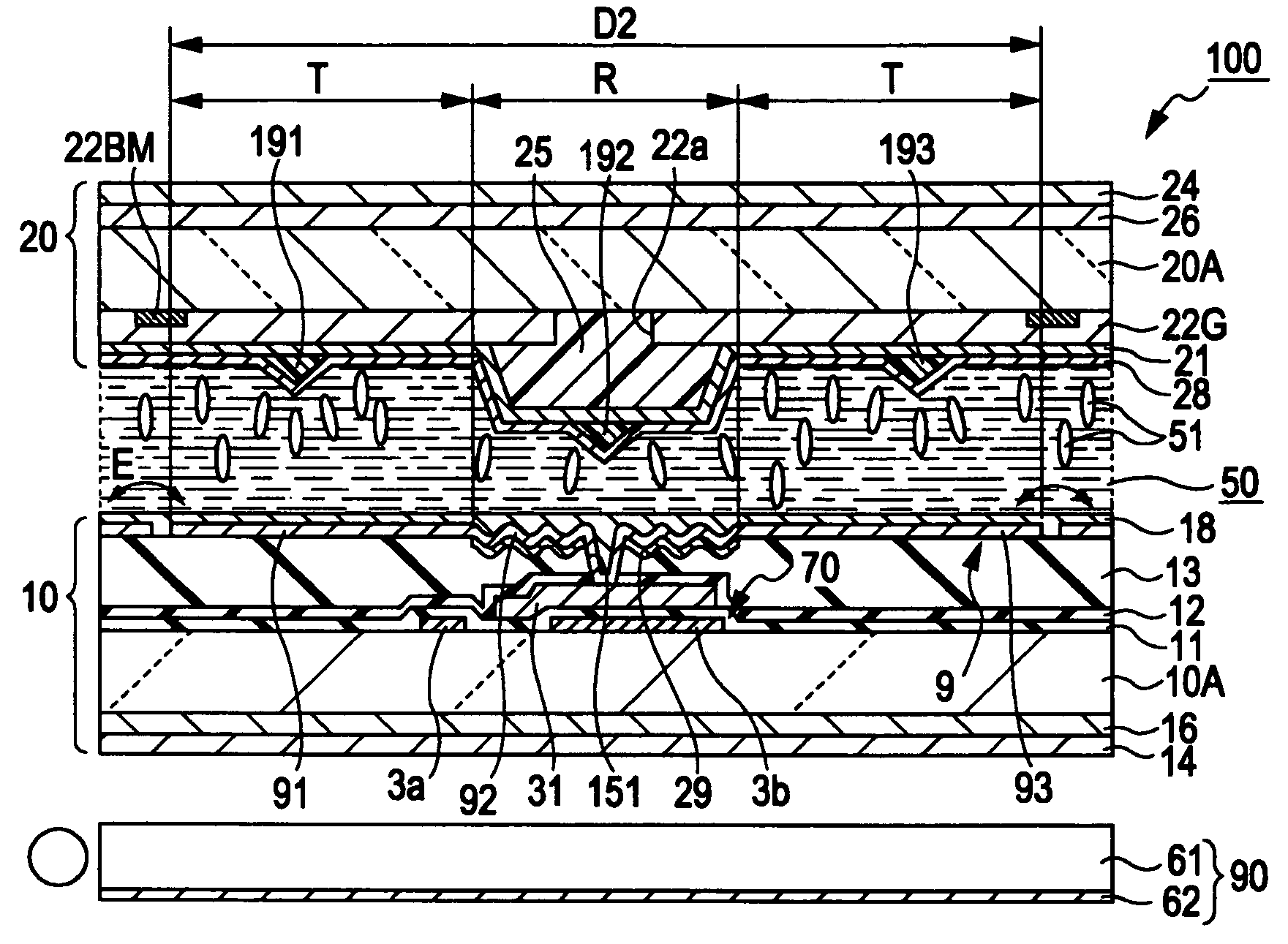
[0033]A liquid crystal device according to a first embodiment of the invention will now be described with reference to the drawings. The liquid crystal device is an active-matrix liquid crystal device of vertically aligned nematic (VAN) mode, including a liquid crystal with negative dielectric anisotropy which is aligned perpendicularly to the surfaces of substrates. The alignment of the liquid crystal is controlled by applying an electric field thereto to perform image display. This liquid crystal device is a transflective liquid crystal device including subpixels having reflective and transmissive display regions. The liquid crystal device has red (R), green (G), and blue (B) color filters (coloring layers) provided on one of the substrates to enable color display. Each pixel includes three subpixels that emit R light, G light, and B light. In the present specification, the term “subpixel” refers to the minimum display unit, and the term “pixel” refers to a display region includin...

second embodiment

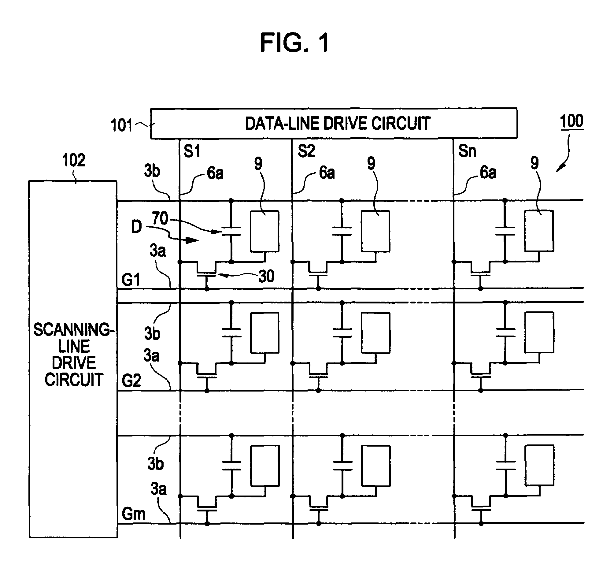
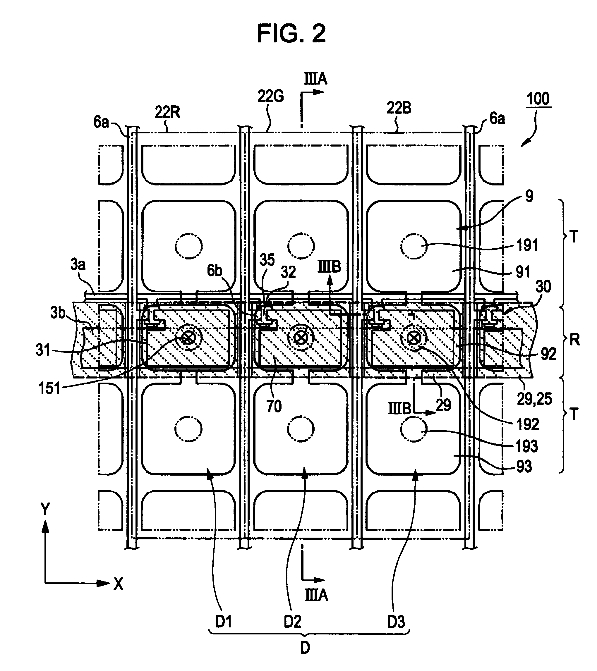
[0062]A liquid crystal device according to a second embodiment of the invention will now be described with reference to FIGS. 5, 6, 7A, and 7B. FIG. 5 is a circuit diagram of the liquid crystal device according to this embodiment. FIG. 6 is a plan view of three subpixels included in any pixel of the liquid crystal device according to this embodiment. FIGS. 7A and 7B are partial sectional views taken along lines VIIA-VIIA and VIIB-VIIB, respectively, in FIG. 6. In FIGS. 5, 6, 7A, and 7B, components similar to those of the liquid crystal device 100 shown in FIGS. 1 to 4 are indicated by the same reference numerals, and the detailed description thereof will be omitted.

[0063]A liquid crystal device 200 according to this embodiment is an active-matrix liquid crystal device including TFDs (two-terminal nonlinear elements) 41. The liquid crystal device 200, as well as the liquid crystal device 100 according to the first embodiment, is a transflective liquid crystal device having a multigap...

third embodiment

[0079]Next, a third embodiment of the invention will be described below with reference to FIG. 8. A liquid crystal device 300 shown in FIG. 8 is a modification of the liquid crystal device 200 according to the second embodiment shown in FIGS. 5, 6, 7A, and 7B. The liquid crystal device 300 differs from the liquid crystal device 200 only in the alignment control members used for controlling the alignment of the liquid crystal layer 50. In FIG. 8, components similar to those of the liquid crystal device 200 according to the second embodiment are indicated by the same reference numerals, and the detailed description thereof will be omitted.

[0080]Referring to FIG. 8, electrode slits 491 to 493 are formed in the counter electrode 3 disposed on the counter substrate 120 of the liquid crystal device 300 by partially removing the counter substrate 120. The electrode slits 491 to 493 are substantially circular in plan view and function to control the alignment of the liquid crystal layer 50....


PUM

PropertyMeasurementUnit
thicknessaaaaaaaaaa
thicknessaaaaaaaaaa
diameteraaaaaaaaaa

Abstract

A liquid crystal device includes a pair of substrates and a liquid crystal layer held between the substrates and containing a liquid crystal having negative dielectric anisotropy. The liquid crystal layer includes subpixels, each including a plurality of transmissive display regions and a reflective display region that are arranged in a predetermined direction. The transmissive display regions are disposed at the ends of each subpixel in the direction in which the transmissive and reflective display regions are arranged. The liquid crystal device further includes a thickness-adjusting layer disposed between at least one of the substrates and the liquid crystal layer so that the liquid crystal layer is thinner in the reflective display region than in the transmissive display regions.

Description

BACKGROUND[0001]1. Technical Field[0002]The present invention relates to liquid crystal devices and electronic apparatuses.[0003]2. Related Art[0004]Among known liquid crystal devices are transflective liquid crystal devices, which operate in both reflective mode and transmissive mode. JP-A-2000-047217, for example, proposes a transflective liquid crystal device having a multigap structure, in which the thickness of a liquid crystal layer differs between reflective display regions and transmissive display regions to enhance contrast. Another type of transflective liquid crystal device includes a homeotropic liquid crystal to improve viewing-angle characteristics (see, for example, “Development of transflective LCD for high contrast and wide viewing angle by using homeotropic alignment”, M. Jisaki et al., Asia Display / ID W'01, pp. 133-136 (2001)).[0005]The homeotropic liquid crystal device above includes protrusions disposed in the centers of transmissive display regions to control t...

Claims


Application Information

Patent Timeline
Patent Type & Authority Patents(United States)
IPC IPC(8): G02F1/1343
CPCG02F1/133555G02F1/133707G02F2001/13712G02F1/13712
Inventor HIGA, MASAKATSUNISHIMURA, JOJI
Owner JAPAN DISPLAY WEST
Why Eureka
Try Eureka