Method of manufacturing complementary metal oxide semiconductor image sensor

a semiconductor and image sensor technology, applied in the direction of semiconductor devices, diodes, radiation control devices, etc., can solve the problems of difficult to be made in a single chip, ccds require high power consumption, and many manufacturing processes

Inactive Publication Date: 2009-09-29
DONGBU ELECTRONICS CO LTD
View PDF6 Cites 29 Cited by
  • Summary
  • Abstract
  • Description
  • Claims
  • Application Information

AI Technical Summary

Problems solved by technology

CCDs require high power consumption and many complicated manufacturing processes and are difficult to be made in a single chip.
However, the conventional CMOS image sensor has the following problems.
This makes it difficult to independently adjust a capacitance value of the floating diffusion (FD) region.

Method used


Image

  • Method of manufacturing complementary metal oxide semiconductor image sensor
  • Method of manufacturing complementary metal oxide semiconductor image sensor
  • Method of manufacturing complementary metal oxide semiconductor image sensor

Examples


Embodiment Construction

[0032]Hereinafter, a complementary metal oxide semiconductor (CMOS) image sensor and a method of manufacturing the same according to preferred embodiments of the present invention will be described with reference to the accompanying drawings.

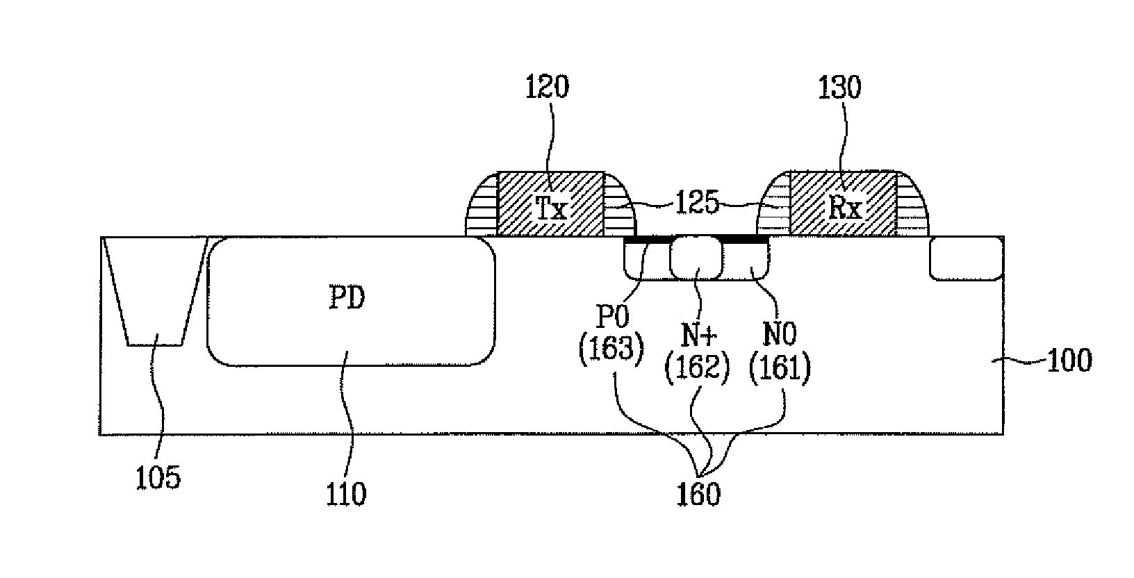
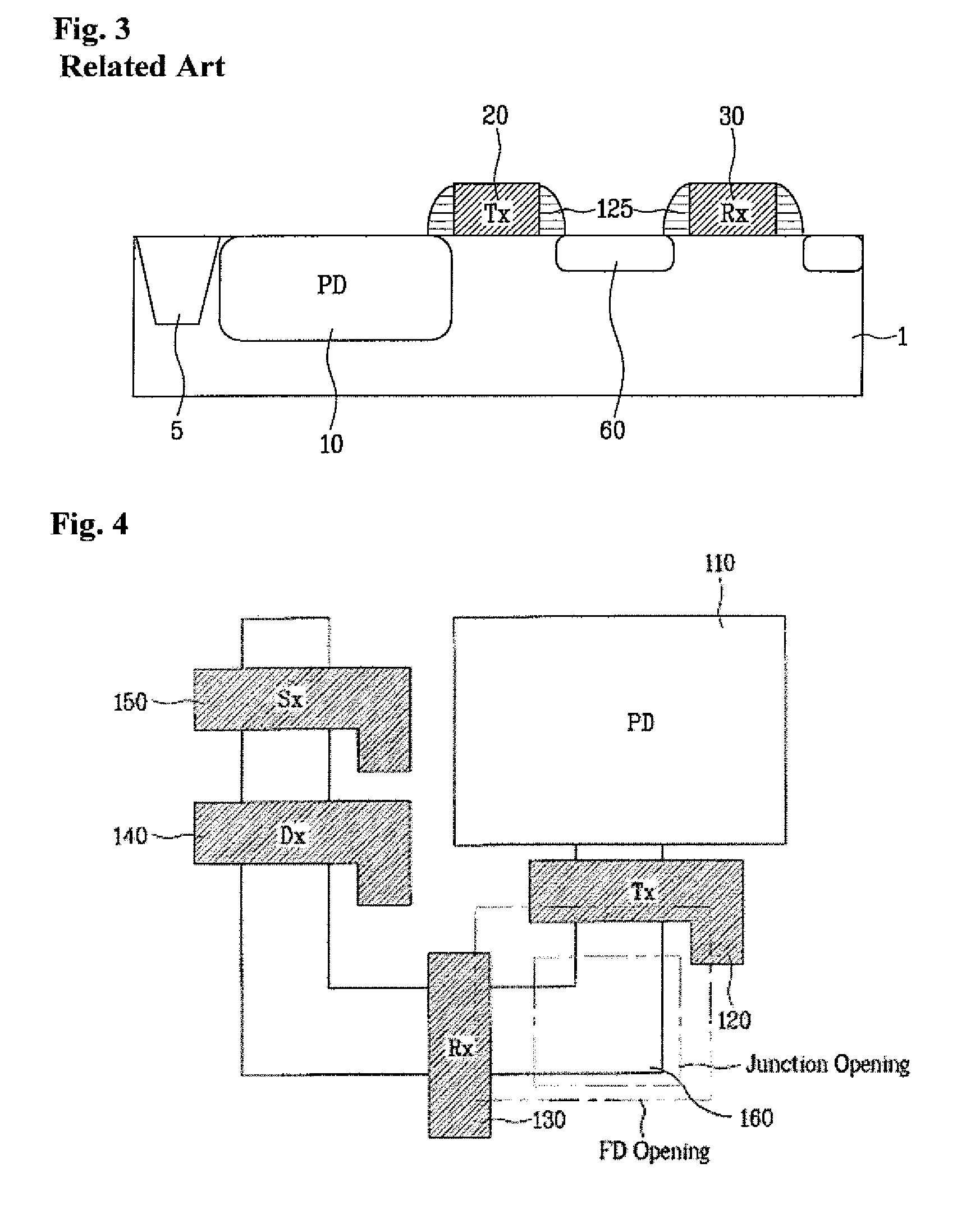
[0033]FIG. 4 is a layout view illustrating a unit pixel of a complementary metal oxide semiconductor (CMOS) image sensor according to an embodiment of the present invention, and FIG. 5 is a sectional view illustrating a CMOS image sensor according to an embodiment of the present invention.

[0034]As illustrated in FIGS. 4 and 5, a CMOS image sensor of the present invention can include a semiconductor substrate 100 having an isolation layer 105, a photodiode 110 formed at a predetermined portion of the semiconductor substrate 100, a plurality of gate polys 120 and 130 formed by the photodiode 110 at a predetermined interval, spacers 125 formed on sidewalls of the gate polys 120 and 130, a floating diffusion region 160 formed between the gate polys ...


PUM


Abstract

A method of manufacturing a complementary metal oxide semiconductor (CMOS) image sensor is provided. The method can include the steps of: providing a semiconductor substrate having an active region and an isolation region defined thereon; forming a photodiode at a photodiode area of the active region; forming first and second gate polys on a transistor region of the active region; forming a floating diffusion region on the semiconductor substrate between the first and second gate polys for receiving electrons transferred from the photodiode; and forming a floating diffusion node region at a part of the floating diffusion region for forming a metal contact. The floating diffusion region can be formed independently of the floating diffusion node region, so that a junction leakage current generated from the floating diffusion node region can be controlled.

Description

RELATED APPLICATION(S)[0001]This application claims priority under 35 U.S.C. §119(e) of Korean Patent Application No. 10-2005-0134174 filed Dec. 29, 2005, which is incorporated herein by reference in its entirety.FIELD OF THE INVENTION[0002]The present invention relates to a method of manufacturing an image sensor. Particularly, the present invention relates to a method of forming a floating diffusion node region of a complementary metal oxide semiconductor (CMOS) image sensor.BACKGROUND OF THE INVENTION[0003]In general, image sensors are semiconductor devices for converting optical images into electric signals, and are generally classified as charge coupled device (CCD) image sensors or complementary metal oxide semiconductor (CMOS) image sensors.[0004]CCDs require high power consumption and many complicated manufacturing processes and are difficult to be made in a single chip.[0005]For this reason, the CMOS image sensor has recently been spotlighted.[0006]The CMOS sensor includes ...

Claims


Application Information

Patent Timeline
Patent Type & Authority Patents(United States)
IPC IPC(8): H01L21/00
CPCH01L27/14603H01L27/14689H01L27/14643H01L27/14609H01L27/146
Inventor SHIM, HEE SUNG
Owner DONGBU ELECTRONICS CO LTD
Why Eureka
Try Eureka