Method of making a circuitized substrate with enhanced circuitry and electrical assembly utilizing said substrate

a technology of enhanced circuitry and electrical assembly, applied in the direction of printed circuit manufacturing, printed circuit aspects, conductive pattern formation, etc., can solve the problems of reliability problems, unsatisfactory conventional gaussian distribution and uniform distribution, and inability to remove dielectrics from holes, etc., and achieve cost-effective effects

Active Publication Date: 2009-09-29
TTM TECH NORTH AMERICA LLC
View PDF15 Cites 49 Cited by
  • Summary
  • Abstract
  • Description
  • Claims
  • Application Information

AI Technical Summary

Benefits of technology

[0016]Accordingly, it is a primary object of this invention to enhance the art of making circuitized substrates and particularly that portion of the art relating to through-hole formation.
[0017]It is another object of this invention to provide such a method which can be cost effectively performed, utilizing, for the most part, conventional circuitized substrate manufacturing equipment.

Problems solved by technology

The use of a multi-layered interconnect structure such as an organic, laminate chip carrier for interconnecting a semiconductor chip to a printed circuit board in an electronic package introduces many challenges.
One of the most significant challenges facing such highly miniaturized products is the challenge to provide the necessary, highly dense circuit patterns able to conduct the high frequency (speed) signals from the positioned chip(s) to the underlying supporting substrate on which the carrier is positioned.
This patent states that it is undesirable to remove dielectric from the hole and hence the reason for leaving the dielectric at the flush level.
This patent further states that conventional Gaussian distribution and uniform distribution are less desirable because these energy distributions tend to remove dielectric material within the opening of the PTH, which may lead to reliability problems caused by entrapped plating solution.

Method used


Image

  • Method of making a circuitized substrate with enhanced circuitry and electrical assembly utilizing said substrate
  • Method of making a circuitized substrate with enhanced circuitry and electrical assembly utilizing said substrate
  • Method of making a circuitized substrate with enhanced circuitry and electrical assembly utilizing said substrate

Examples


Embodiment Construction

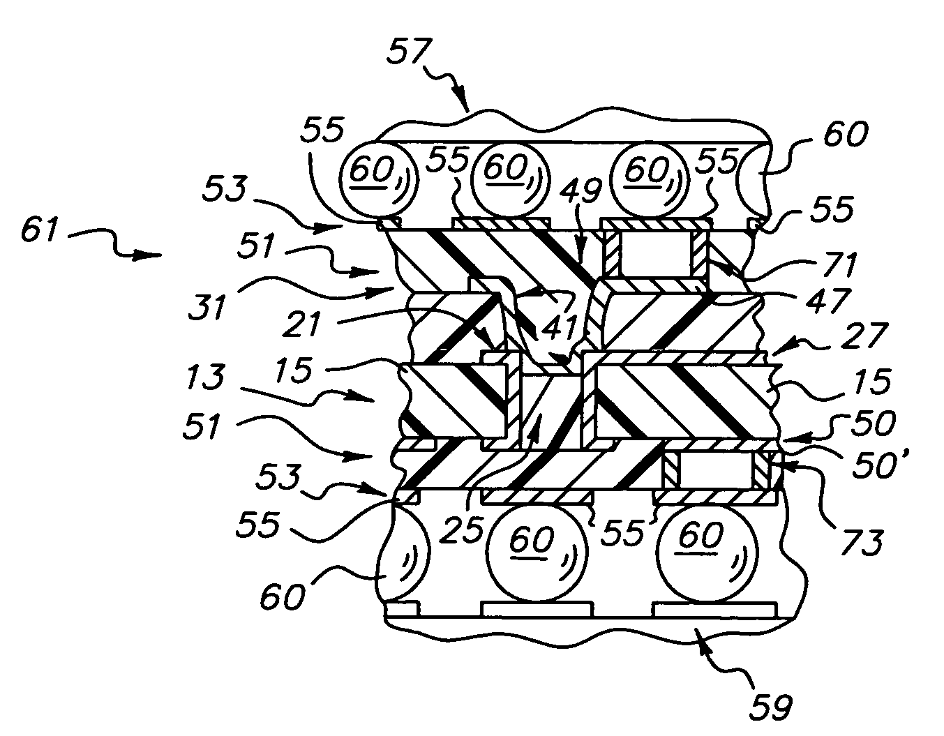
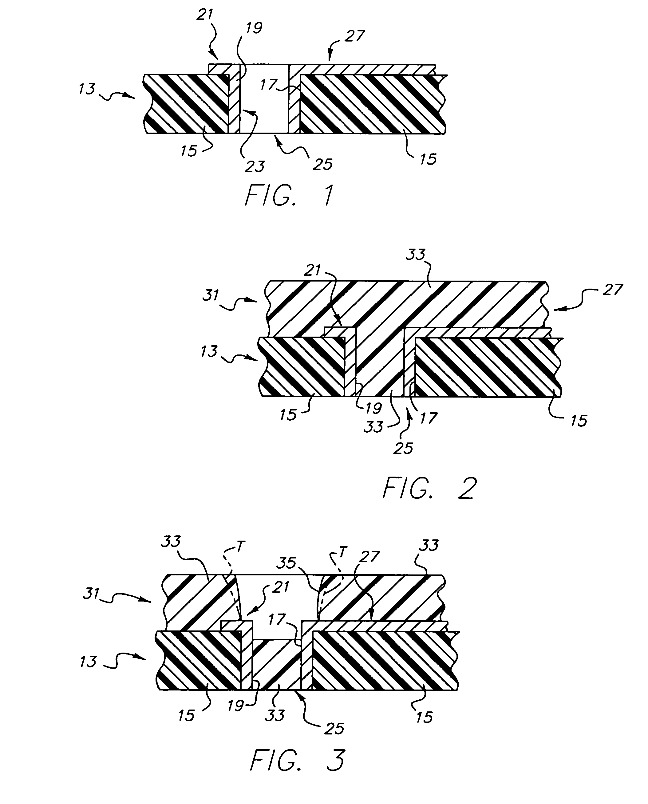
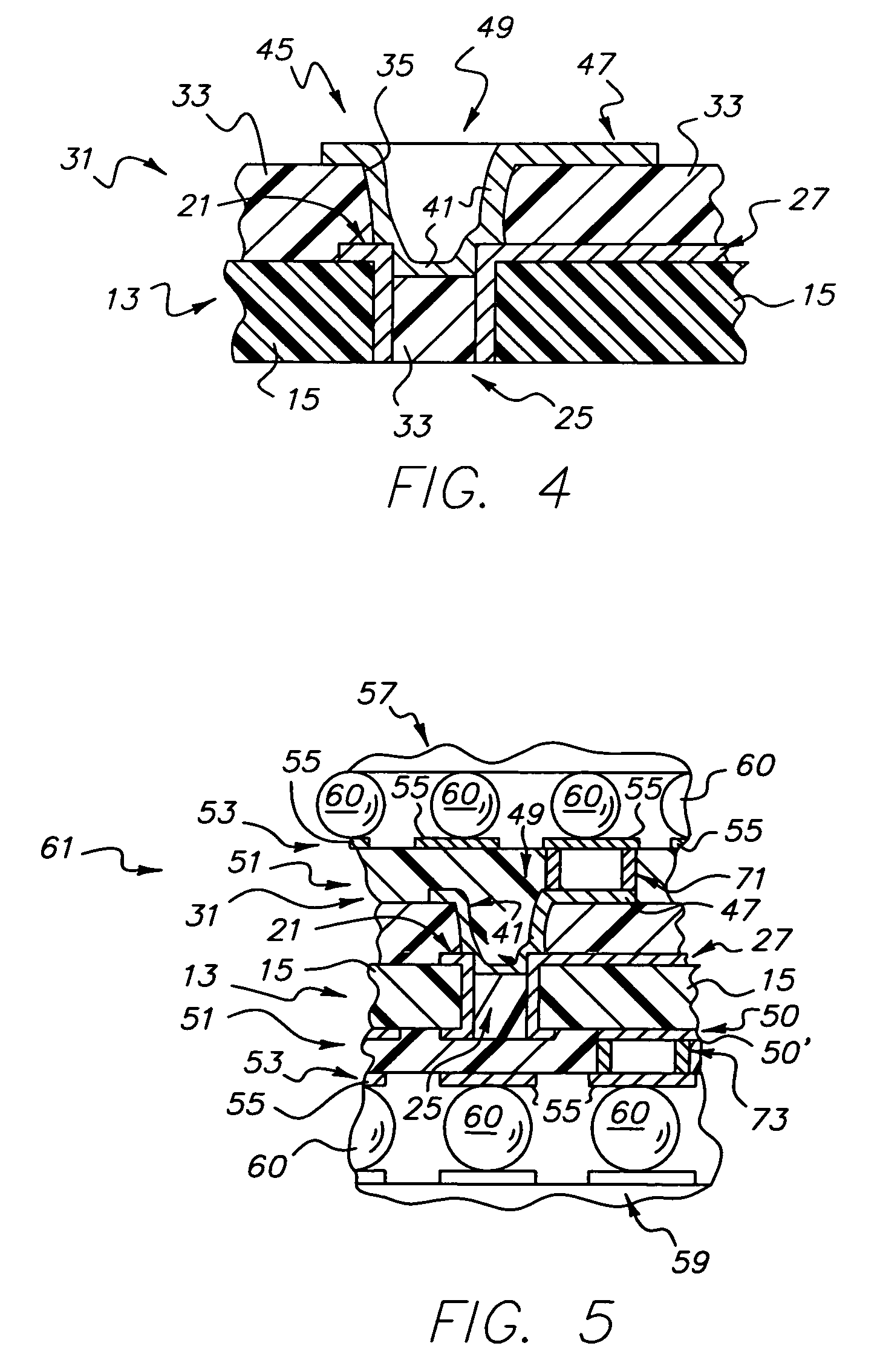
[0023]For a better understanding of the present invention, together with other and further objects, advantages and capabilities thereof, reference is made to the following disclosure and appended claims in connection with the above-described drawings. It is understood that like numerals will be used to indicate like elements from FIG. to FIG.

[0024]By the term “circuitized substrate” as used herein is meant to include substrates having at least two (and preferably more) dielectric layers and at least three (and preferably more electrically conductive layers, these layers being typically arranged in an alternating manner. Examples of dielectric materials usable for such substrates include fiberglass-reinforced epoxy resins (some referred to as “FR4” dielectric materials in the art, for the flame retardant rating of same), polytetrafluoroethylene (e.g., Teflon), polyimides, polyamides, cyanate resins, photo-imageable materials and other like materials. Examples of conductor materials u...


PUM

PropertyMeasurementUnit
widthaaaaaaaaaa
widthaaaaaaaaaa
widthaaaaaaaaaa

Abstract

A method of making a circuitized substrate in which pairs of vertically oriented though holes are formed such that at least one of the through holes is partially embedded within a lower one, thus assuring a sound connection following subsequent lamination or other steps the substrate including such holes is subjected to during manufacture. An electrical assembly including a substrate with such features is also provided.

Description

TECHNICAL FIELD[0001]The present invention relates, in general, to methods of making circuitized substrates such as printed circuit boards (hereinafter also referred to as PCB's), chip carriers and the like. Even more particularly, the invention relates to such methods designed for providing highly dense circuit patterns such that the substrates produced using the teachings herein will comply with today's demanding operational requirements for the products utilizing same. One example of such a product is known in the art as an electronic package.BACKGROUND OF THE INVENTION[0002]Electronic packages and similar products which include organic laminate substrates have been and continue to be developed for many of today's applications. One primary example of such a product is a chip carrier sold under the name HyperBGA by the Assignee of this invention, Endicott Interconnect Technologies, Inc. (HyperBGA is a registered trademark of Endicott Interconnect Technologies, Inc.) These carriers...

Claims


Application Information

Patent Timeline
Patent Type & Authority Patents(United States)
IPC IPC(8): H01R12/14
CPCH05K1/115H05K3/421H05K3/4602H05K2201/09536Y10T29/49155H05K2201/096Y10T29/49165Y10T29/49126H05K2201/0959
Inventor KRESGE, JOHN S.PALOMAKI, CHERYL L.
Owner TTM TECH NORTH AMERICA LLC
Why Eureka
Try Eureka