

MOS type semiconductor device having electrostatic discharge protection arrangement
a technology of protection arrangement and semiconductor device, which is applied in the direction of semiconductor device, semiconductor/solid-state device details, electrical apparatus, etc., can solve the problems of difficulty in simultaneously solving both the uneven snapback-occurrence problem
- Summary
- Abstract
- Description
- Claims
- Application Information
AI Technical Summary
Benefits of technology
Problems solved by technology
Method used
Image

Examples
first embodiment
[0085]With reference to FIGS. 9 to 12, a first embodiment of a MOS type semiconductor device having an ESD protection arrangement according to the present invention is explained below.
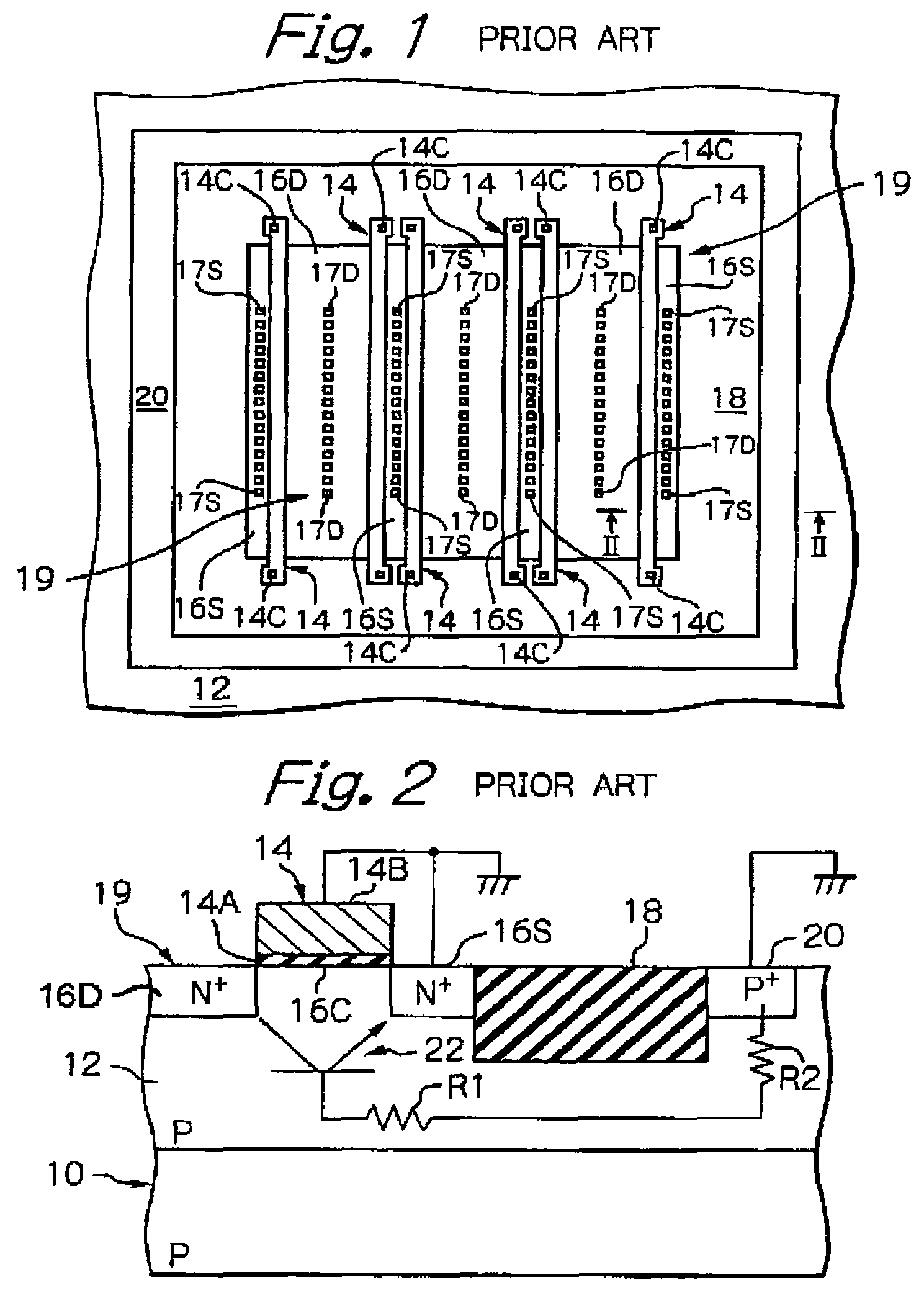
[0086]As shown in FIG. 10, the MOS type semiconductor device includes a P-type semiconductor substrate 40, which is derived from, for example, a P-type silicon wafer. As is apparent from FIGS. 9 and 10, a P-type well region 41P is formed in the P-type semiconductor substrate 40, and an N-type well region 41N is formed in the P-type well region 41P. Also, a rectangular transistor-formation area 42P is defined in the P-type well region 41P by forming an STI layer 43P therein, and a rectangular transistor-formation area 42N is defined in the N-type well region 31N by forming an STI layer 43N therein.
[0087]The MOS type semiconductor device features a multi-finger structure for effectively constituting the ESD protection arrangement.
[0088]In particular, at the transistor-formation area 42P, a plurality of e...
second embodiment
[0117]FIGS. 14 and 15 shows a second embodiment of the MOS type semiconductor device having the ESD protection arrangement according to the present invention. Note, in FIGS. 14 and 15, the features similar to those of FIGS. 9 and 12 are indicated by the same references.
[0118]This second embodiment is substantially identical to the above-mentioned first embodiment except that a gap 54 is formed in the STI layer 43P at the center of the side 51 of the transistor-formation area 42P which is adjacent to the transistor-formation area 42N, and the guard-ring 48P has a protrusion 48PP integrally extended therefrom into the gap 54.
[0119]In this second embodiment, it is possible to make the substrate resistance (RSUD / GAP) smaller between the transistor-formation area 42P and the guard-ring 48P, due to the existence of the protrusion 48PP formed as a part of the guard-ring 48P, and thus the occurrence of the snapbacks in all the fingers F1 to F6 can be further securely ensured.
[0120]Also, acc...
third embodiment
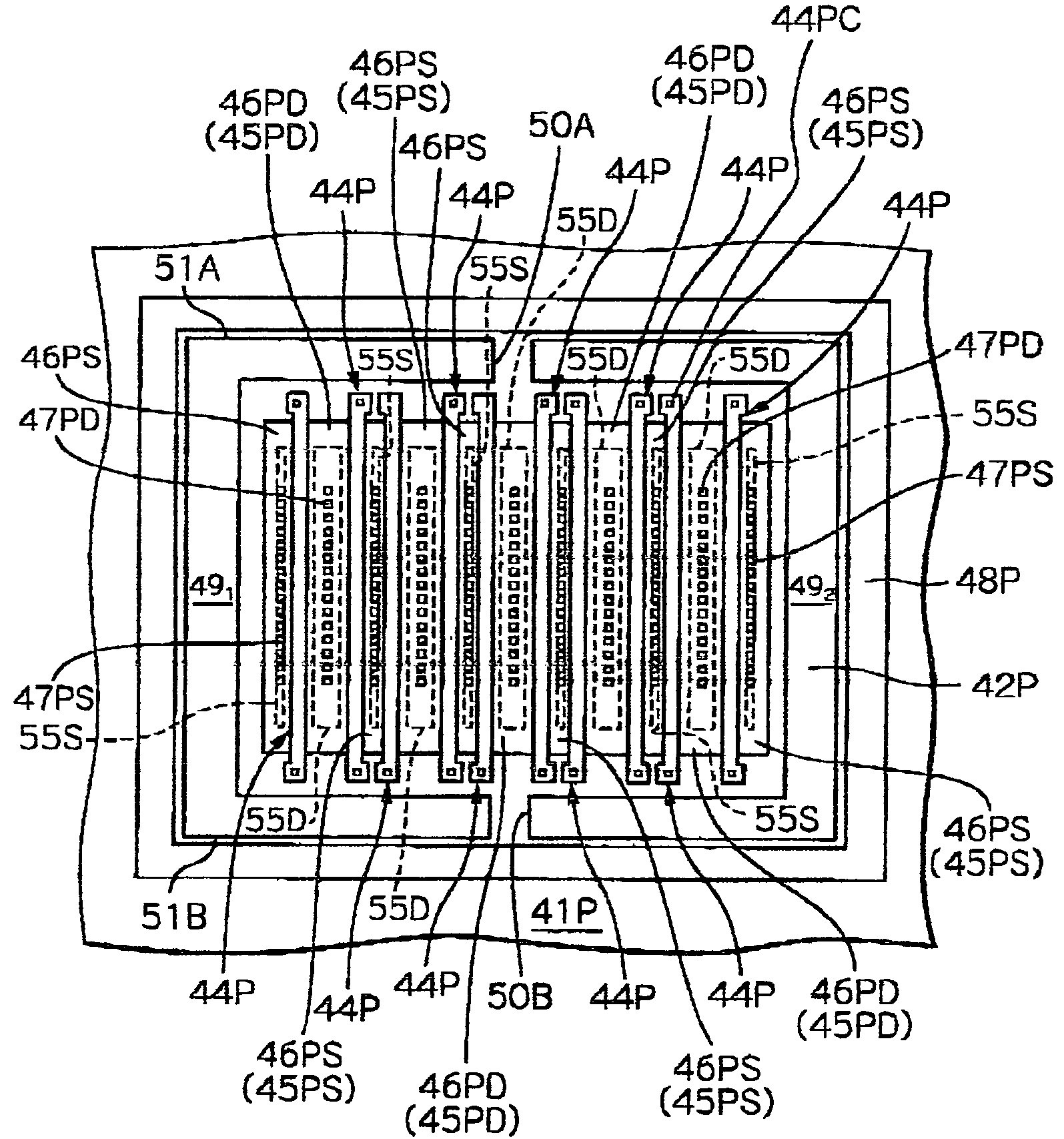
[0122]FIG. 16 shows a third embodiment of the MOS type semiconductor device having the ESD protection arrangement according to the present invention. Note, in FIG. 16, the features similar to those of FIG. 9 are indicated by the same references.
[0123]In FIG. 16, only an ESD protection device defined in a rectangular transistor-formation area 42P is illustrated, and an STI layer (43P) is eliminated from FIG. 16 to directly illustrate a pair of P-type well blocking regions 491 and 492 by solid lines.
[0124]In the third embodiment, the ESD protection device features a multi-finger structure including ten fingers, and each of the fingers includes an elongated gate electrode 44P, and source and drain regions 45PS and 45PD arranged along the respective sides of the elongated gate electrode 44P concerned. Each of the source regions 45PS is covered with a silicide layer 46PS formed thereon. Similarly, each of the drain regions 45PS is covered with a silicide layer 47PD formed thereon. Note, ...
PUM
 Abstract
Description
Claims
Application Information