Multi-stage charge pump without threshold drop with frequency modulation between embedded mode operations

a charge pump and frequency modulation technology, applied in the direction of dc-dc conversion, power conversion systems, instruments, etc., can solve problems such as significant voltage loss, and achieve the effects of saving area, reducing the number of capacitors needed, and optimizing power efficiency

Active Publication Date: 2009-09-29
MACRONIX INT CO LTD
View PDF14 Cites 85 Cited by
  • Summary
  • Abstract
  • Description
  • Claims
  • Application Information

AI Technical Summary

Benefits of technology

[0014]Embodiments of the multimode charge pump described herein include a precharge circuit coupled to at least one corresponding stage, operable in the first mode in a manner that enables transfer of higher voltages from previous stages to the corresponding stage in the multimode charge pump, and operable in the second mode in a manner that couples the input supply potential to the corresponding stage, without significant voltage loss, by for example using a PMOS transistor having a drain coupled to a source of the supply potential, and with low voltage applied to its gate, and disables transfer of higher voltages to the corresponding stage from preceding stages. A significant voltage loss in this context is a voltage loss on the order of a threshold drop from a transistor operating in the linear mode.
[0015]A precharge circuit is described which includes a first PMOS transistor having a source terminal coupled to a source of the supply potential, a drain terminal coupled to the supply node, and a gate; a second PMOS transistor having a source terminal coupled to the source node, a drain terminal coupled to the gate of the first PMOS transistor, and a gate coupled to a control node; and an NMOS transistor having a source terminal coupled to a reference supply, a drain terminal coupled to the gate of the first PMOS transistor, and a gate coupled to the control node. The first PMOS transistor is biased on with low voltage at is gate, when the control node is at a high potential, and transfers the supply potential to the supply node without significant voltage loss.
[0018]One or more precharge circuits, having first and second states as described above, are coupled respectively to the supply nodes of one or more of the intermediate stages and the last stage. The precharge circuits are utilized to configure the plurality of charge pump stages, by applying control signals that cause the precharge circuit connected to a corresponding intermediate stage to enter the second state, while causing the precharge circuits coupled to the following stages to enter the first state. In this manner, the intermediate stage coupled to the precharge circuit in the second state, becomes the input stage for the charge pump, and is able to receive a supply potential as input, via a transistor for example, substantially without voltage drop.
[0020]The technology described herein provides charge pump technology which is configurable for operation in multimode environments, including the use of different clocks for different modes and the use of different numbers of charge pump stages in different modes. The charge pump technology therefore allows for optimized power efficiency and a reduction in the number of capacitors needed on a single integrated circuit having multiple charge pump modes.
[0021]The charge pump technology described herein is adapted for flash memory, including floating gate memory technology and other charge storage technologies like nitride read-only memory. Flash memory devices typically have a read and standby mode requiring fast response times over a wide temperature range but relatively lower charge pump output voltage, and a program or erase mode requiring higher charge pump output voltage and consistent output over varying supply voltages for programming and erasing operations such as channel hot electron injection and band-to-band tunneling induced hot hole injection. The charge pump technology described herein is suited for providing these modes of operation using a single charge pump, saving area on the integrated circuit and providing more efficient power operation.

Problems solved by technology

A significant voltage loss in this context is a voltage loss on the order of a threshold drop from a transistor operating in the linear mode.

Method used


Image

  • Multi-stage charge pump without threshold drop with frequency modulation between embedded mode operations
  • Multi-stage charge pump without threshold drop with frequency modulation between embedded mode operations
  • Multi-stage charge pump without threshold drop with frequency modulation between embedded mode operations

Examples


Embodiment Construction

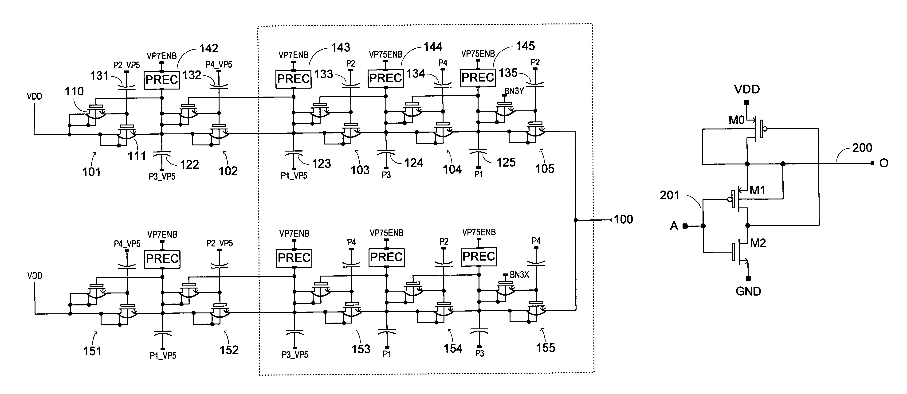
[0040]A detailed description of embodiments of the disclosed technology is provided with reference to the FIGS. 2-19.

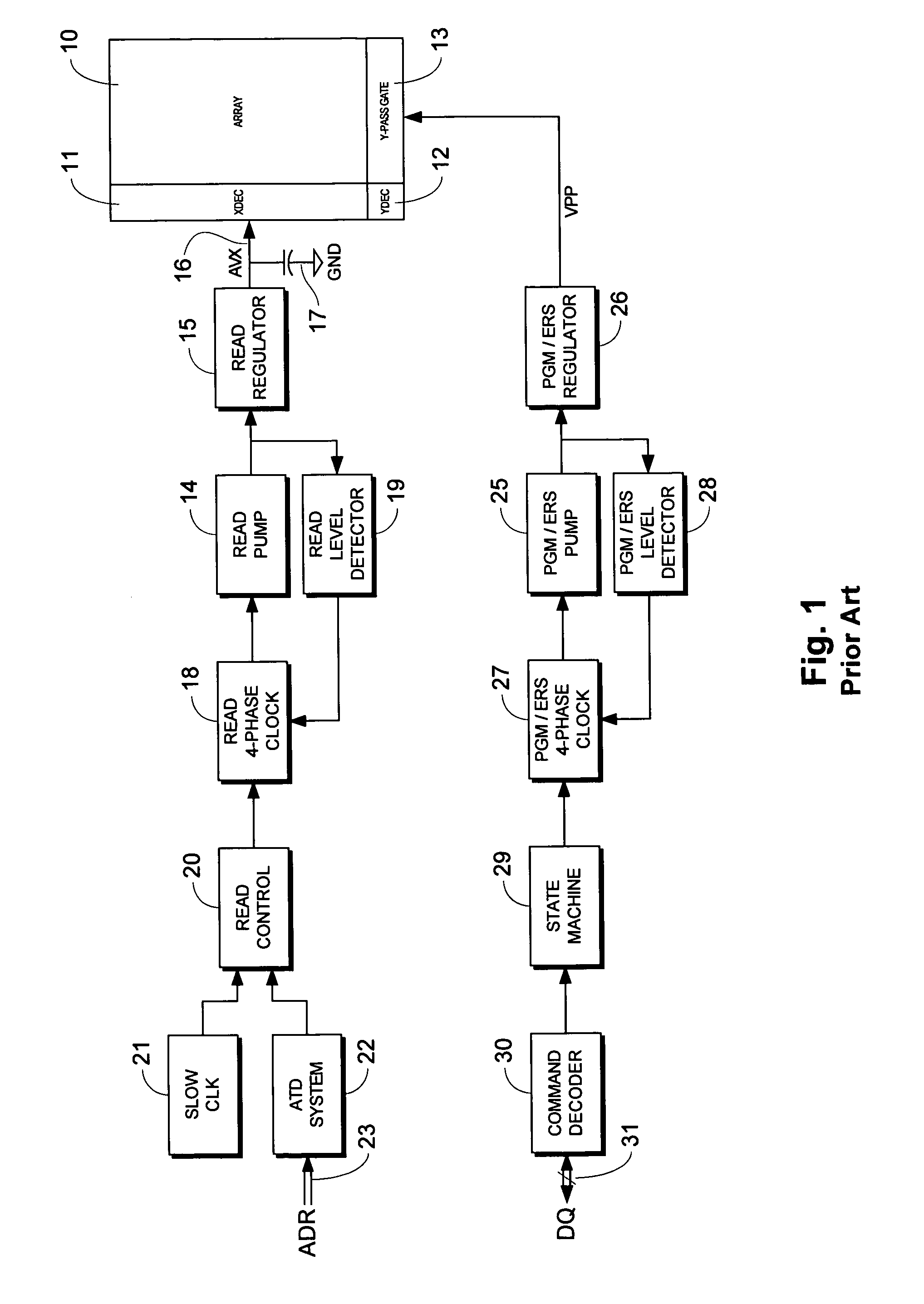
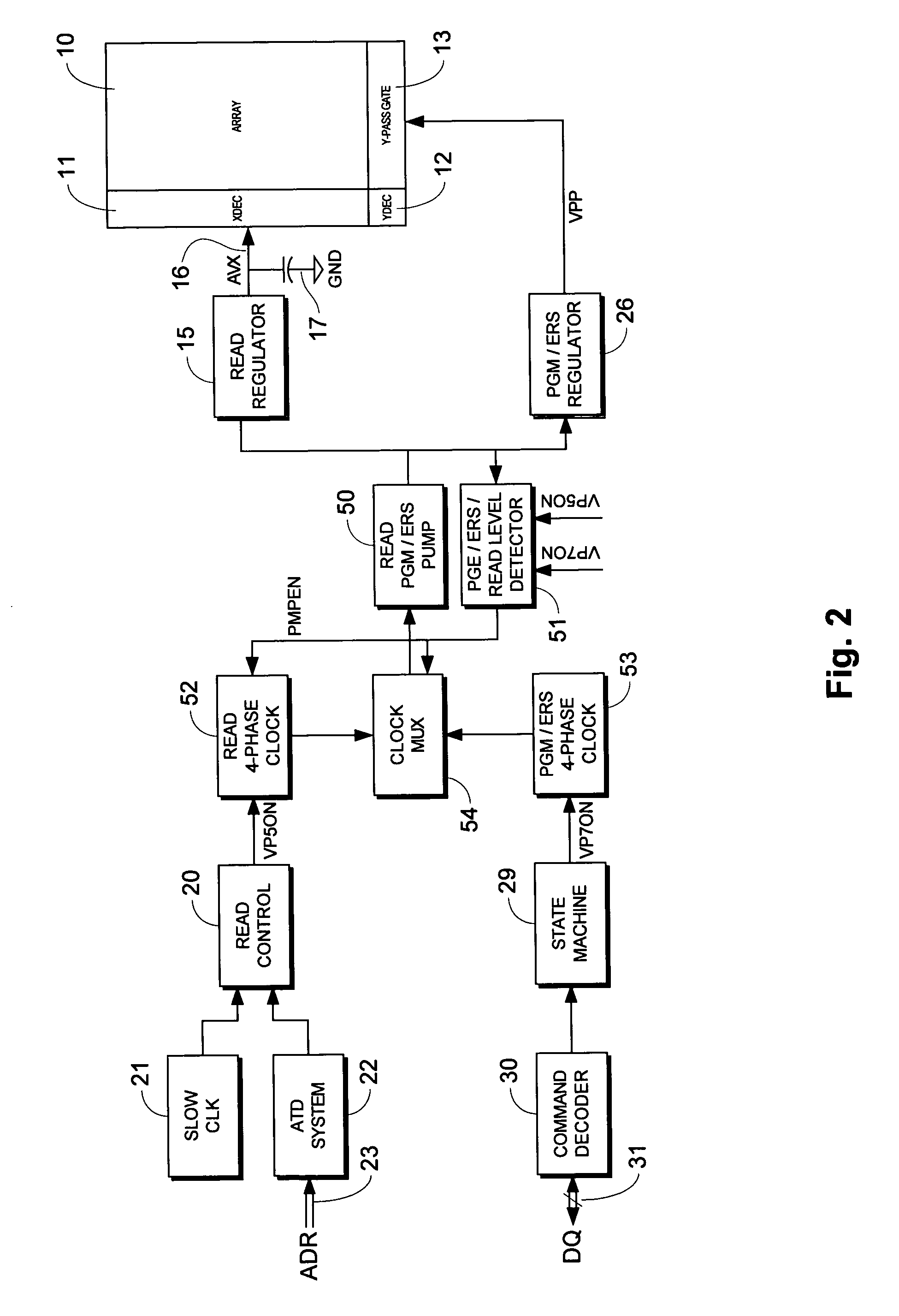
[0041]FIG. 2 shows an embodiment of an integrated circuit with multiple modes and a high-efficiency, multiple mode charge pump, which can be contrasted with the prior art shown in FIG. 1, where like reference numbers identify similar circuitry and are not described again. In the embodiment of FIG. 2, a single charge pump 50 has its output coupled to both the read regulator 15 and PGM / ERS mode regulator 26, replacing the first pump 14 and second charge pump 25 of FIG. 1. Also, a single level detector 51 provides feedback for both modes of operation. A clock source for the charge pump 50 comprises a first read clock 52, a second program / erase clock 53 and a clock multiplexer 54 operable to couple either the output of the first read clock or the output of the second program / erase clock 53 to the charge pump 50. The circuitry implementing the multimode charge pump in FIG....


PUM


Abstract

A multimode charge pump circuit has a single charge pump that is responsive to a set of clock signals. The set of clock signals is provided in a first mode with a variable frequency according to a first function of the supply potential and temperature, and in a second mode with a variable frequency according to a second function of the supply potential and temperature. Circuitry configures all of the plurality of stages in series during the first mode in order to produce a higher voltage output, and configures a subset of the plurality of stages in series, while disabling the other stages, during the second mode in order to produce a lower voltage output. A precharge circuit is provided that operates as a supply node in the second mode, and as a precharge / clamp in the first mode.

Description

BACKGROUND OF THE INVENTION[0001]1. Field of the Invention[0002]The present invention relates to charge pump circuitry, including charge pump circuitry used in integrated circuits having multiple modes of operation.[0003]2. Description of Related Art[0004]Charge pumps are used in integrated circuit design to provide negative voltages, and positive voltages higher than a supply potential available to the integrated circuit. In some integrated circuits, more than one charge pump is required to serve different modes of operation on the integrated circuit, or to serve different circuit modules on the integrated circuit. The charge pumps on the integrated circuit are adapted for the particular mode of operation or circuit module so that performance of the charge pump meets the needs of the load being driven in such parameters as output voltage level, output current level and responsiveness.[0005]For example, in integrated circuit devices including flash memory, a first charge pump can be...

Claims


Application Information

Patent Timeline
Patent Type & Authority Patents(United States)
IPC IPC(8): G05F1/10
CPCH02M3/073H02M2003/075H02M3/075
Inventor LIN, YUFE FENGLIN, YU SHENCHEN, ROGERHUNG, CHUN HSIUNG
Owner MACRONIX INT CO LTD
Why Eureka
Try Eureka