Test structures for stacking dies having through-silicon vias

a technology of silicon vias and test structures, which is applied in the direction of semiconductor/solid-state device testing/measurement, semiconductor device details, semiconductor/solid-state device testing/measurement, etc., can solve the problem of reducing the size of the minimum required to make these components, requiring more complex designs, and physical limitations of the density that can be achieved in two dimensions, etc. problem, to achieve the effect of reducing the complexity of the probing process and increasing the ability to d

Inactive Publication Date: 2009-10-06
TAIWAN SEMICON MFG CO LTD
View PDF3 Cites 50 Cited by
  • Summary
  • Abstract
  • Description
  • Claims
  • Application Information

AI Technical Summary

Benefits of technology

[0013]The advantageous features of the embodiments of the present invention include reducing complexity in the probing process of the stacked dies and increasing the ability to detect the direction and the magnitude of misalignments.

Problems solved by technology

Although dramatic improvement in lithography has resulted in considerable improvements in 2D integrated circuit formation, there are physical limitations to the density that can be achieved in two dimensions.
One of these limitations is the minimum size needed to make these components.
Also, when more devices are put into one chip, more complex designs are required.
Merging these test programs thus becomes a very challenging task.

Method used


Image

  • Test structures for stacking dies having through-silicon vias
  • Test structures for stacking dies having through-silicon vias
  • Test structures for stacking dies having through-silicon vias

Examples


Embodiment Construction

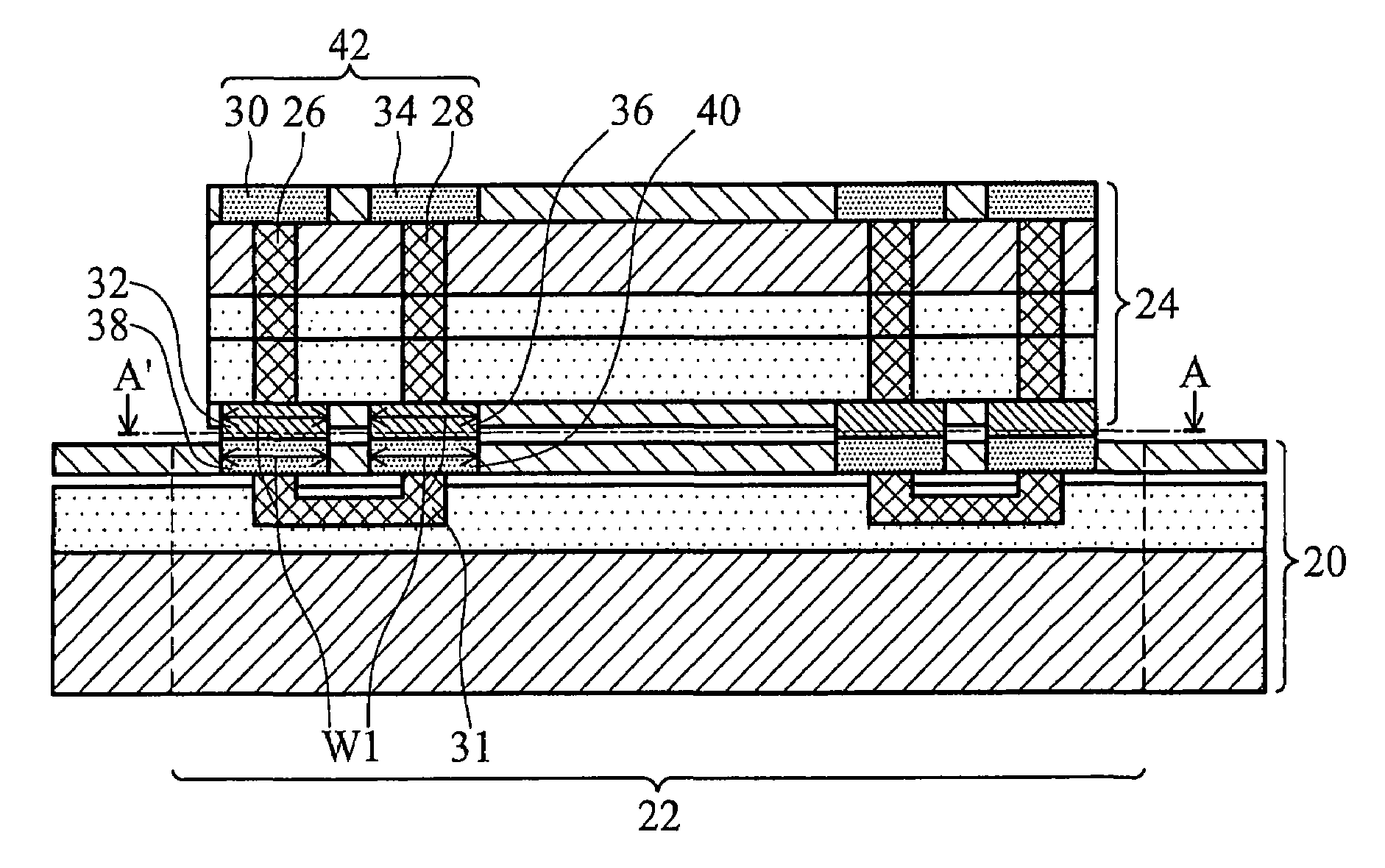
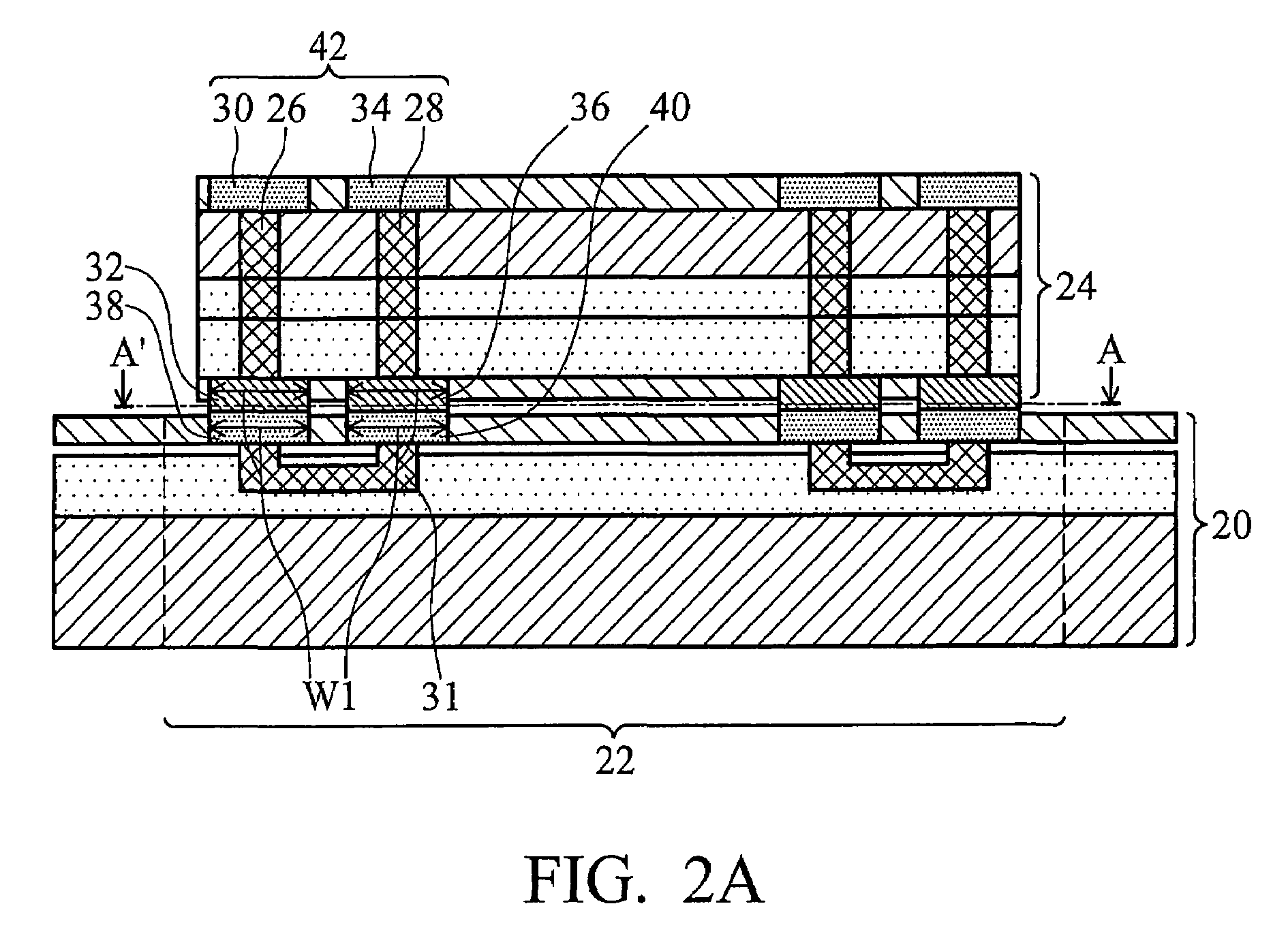
[0021]The making and using of the presently preferred embodiments are discussed in detail below. It should be appreciated, however, that the present invention provides many applicable inventive concepts that can be embodied in a wide variety of specific contexts. The specific embodiments discussed are merely illustrative of specific ways to make and use the invention, and do not limit the scope of the invention.

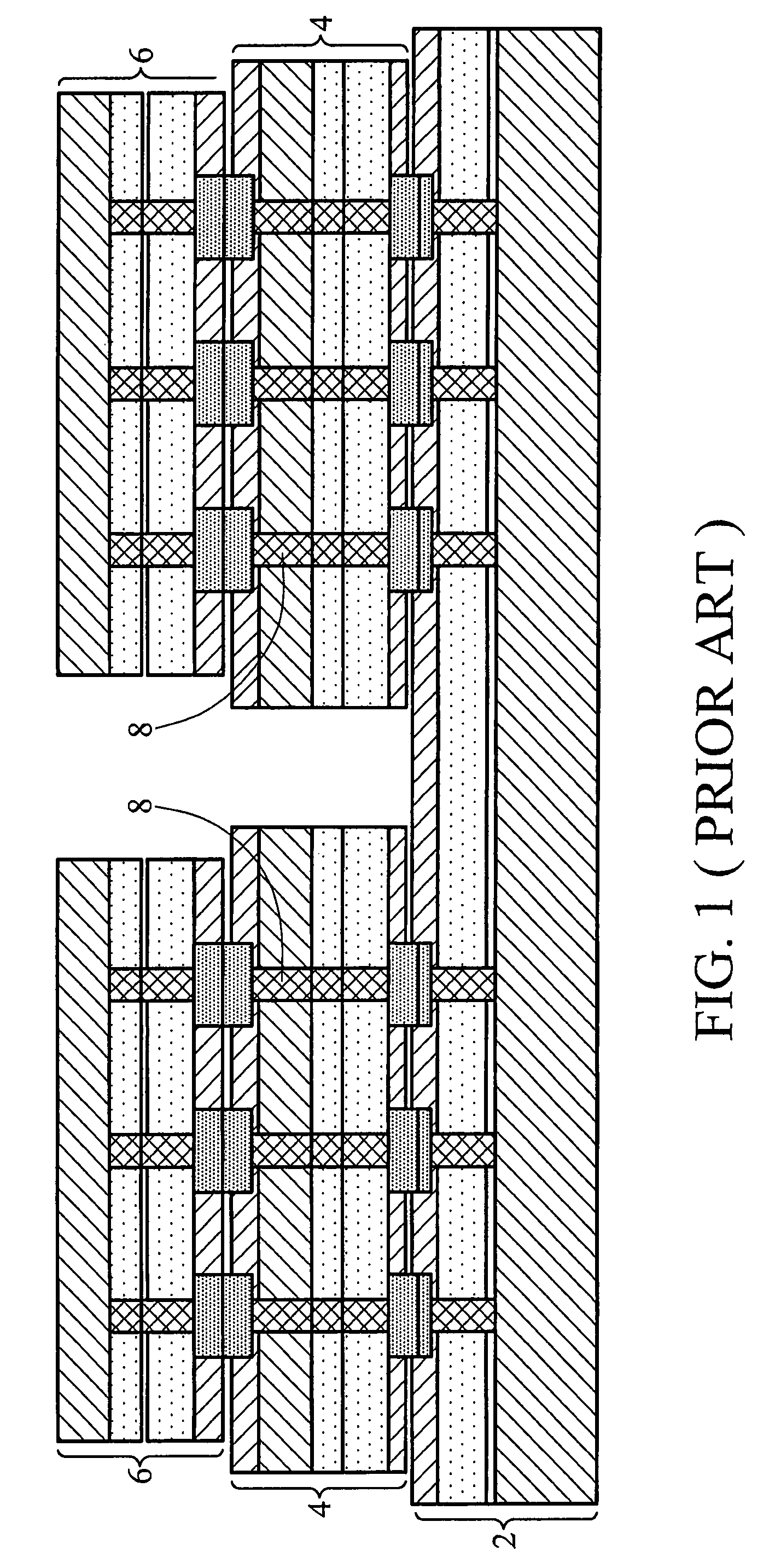
[0022]Typically, before bonding dies and / or wafers, dies on wafers are probed and sorted. Dies designated to be bonded with wafers are also probed and sorted. Only dies passing the probing process are bonded onto the wafers. If some dies on wafers do not pass the probing process, dummy dies will be bonded on the problematic dies on wafers. Therefore, the dies that are bonded and probed (except dummy dies) after stacking are known-good-dies. It can thus be reasonably expected that the stacked dies will function correctly if the stacking process is performed without any misalig...


PUM


Abstract

A semiconductor die including a test structure is provided. The semiconductor die includes a loop-back formed on a surface of the semiconductor die. The loop-back structure includes a first bonding pad on a first surface; and a second bonding pad on the first surface, wherein the first and the second bonding pads are electrically disconnected from integrated circuit devices in the semiconductor die. A conductive feature electrically shorts the first and the second bonding pads. An additional die including an interconnect structure is bonded onto the semiconductor die. The interconnect structure includes a third and a fourth bonding pad bonded to the first and the second bonding pads, respectively. Through-wafer vias in the additional die are further connected to the third and fourth bonding pads.

Description

TECHNICAL FIELD[0001]This invention relates generally to integrated circuits, and more particular to manufacturing and packaging techniques for stacking semiconductor dies having through-silicon vias.BACKGROUND[0002]Since the invention of integrated circuits, the semiconductor industry has experienced a continuous rapid growth due to constant improvements in the integration density of various electronic components (i.e., transistors, diodes, resistors, capacitors, etc.). For the most part, this improvement in integration density has come from repeated reductions in minimum feature size, which allows for more components to be integrated into a given chip area.[0003]These integration improvements are essentially two-dimensional (2D) in nature, in that the volume occupied by the integrated components is essentially on the surface of the semiconductor wafer. Although dramatic improvement in lithography has resulted in considerable improvements in 2D integrated circuit formation, there a...

Claims


Application Information

Patent Timeline
Patent Type & Authority Patents(United States)
IPC IPC(8): H01L29/10
CPCH01L22/34H01L25/0657H01L23/481H01L2225/06596H01L2225/06513H01L2225/06517H01L2225/06541H01L2224/16145H01L2224/05009H01L2224/0557H01L2224/05001H01L2924/00014H01L2224/05571H01L24/05H01L2224/05599
Inventor LUO, WEN-LIANGKUO, YUNG-LIANGCHENG, HSU MING
Owner TAIWAN SEMICON MFG CO LTD
Why Eureka
Try Eureka