Implementation of a metal barrier in an integrated electronic circuit

a technology of integrated electronic circuits and metal barriers, which is applied in the direction of solid-state device manufacturing, electric devices, semiconductor/solid-state device manufacturing, etc., can solve the problems of insufficient prevention of copper atom diffusion across the barrier, the tendency of cobalt-based metal barriers to oxidize, etc., and achieve the effect of improving the anti-oxidation properties of the metal barrier

Active Publication Date: 2009-10-13
STMICROELECTRONICS SRL
View PDF4 Cites 53 Cited by
  • Summary
  • Abstract
  • Description
  • Claims
  • Application Information

AI Technical Summary

Benefits of technology

[0024]In one advantage of this embodiment, the process allows for the formation of metal barriers which are self-aligning.
[0025]The copper atom diffusion blocking (for example) and antioxidation properties of the metal barrier are improved, even in comparison to a metal barrier which is silicided or nitrided but not both at once.

Problems solved by technology

These barriers prevent the diffusion of atoms from the conductive zone to the insulating zone, which can be the origin of integrated circuit malfunctions such as short-circuits between metal lines.
In practice, however, a cobalt-based metal barrier tends to oxidize, particularly when it is exposed to ambient oxidants during later steps involving the deposition of a dielectric material, the plasma etching of this material, etc., as the semiconductor fabrication process continues.
These undesired oxidations can result in:an increase in the electrical resistance of the material forming the metal barrier, and therefore an increase in the electrical resistance of the vias,a decrease in the antidiffusion properties of the metal barrier preventing the diffusion of copper atoms,the formation of voids when wet cleaning is performed after plasma etching the via; such cleaning is well known to a person skilled in the art, and is intended to remove the polymer residues formed during the etching step, particularly at the edge of the vias; however, such cleaning may cause the removal of the Co-M, particularly if it is in oxidized form (Co-M-Ox), and create voids (labeled with the number 19 in the diagram in FIG. 2) which can result in integrity failure of the metal cap 17, appearing as a flaw in said cap (designated by the circle 20 in the diagram in FIG. 2), anda decrease in performance in terms of electromigration.
However, even after the incorporation of silicon atoms by a silicidation process, the cobalt-based metal compound Co-M continues to undergo some oxidation (although to a lesser extent) in the context described above, and the diffusion of copper atoms across this barrier is not completely prevented either.

Method used


Image

  • Implementation of a metal barrier in an integrated electronic circuit
  • Implementation of a metal barrier in an integrated electronic circuit
  • Implementation of a metal barrier in an integrated electronic circuit

Examples


Embodiment Construction

in Semiconductor Products

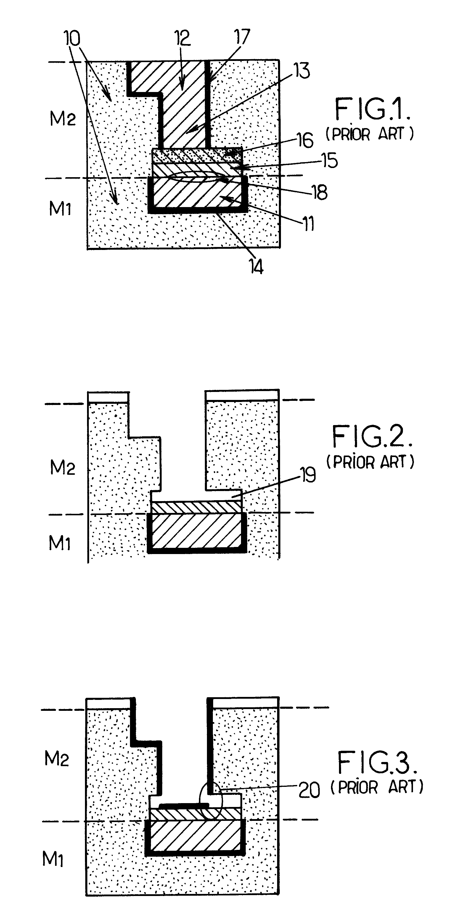
[0080]FIGS. 8 and 9 show examples of semiconductor products comprising self-aligned metal barriers obtained according to embodiments of the invention.

[0081]FIG. 8 shows an interconnect structure comprising a plurality of metallization levels M1, M2 and M3. Each of the metallization levels of the interconnect structure comprises, for example, a layer of undoped silicon glass (USG) in which is realized at least one conductive line 96 which is of copper, for example.

[0082]Conductive lines 96 in separate metallization levels can be connected by vias 97.

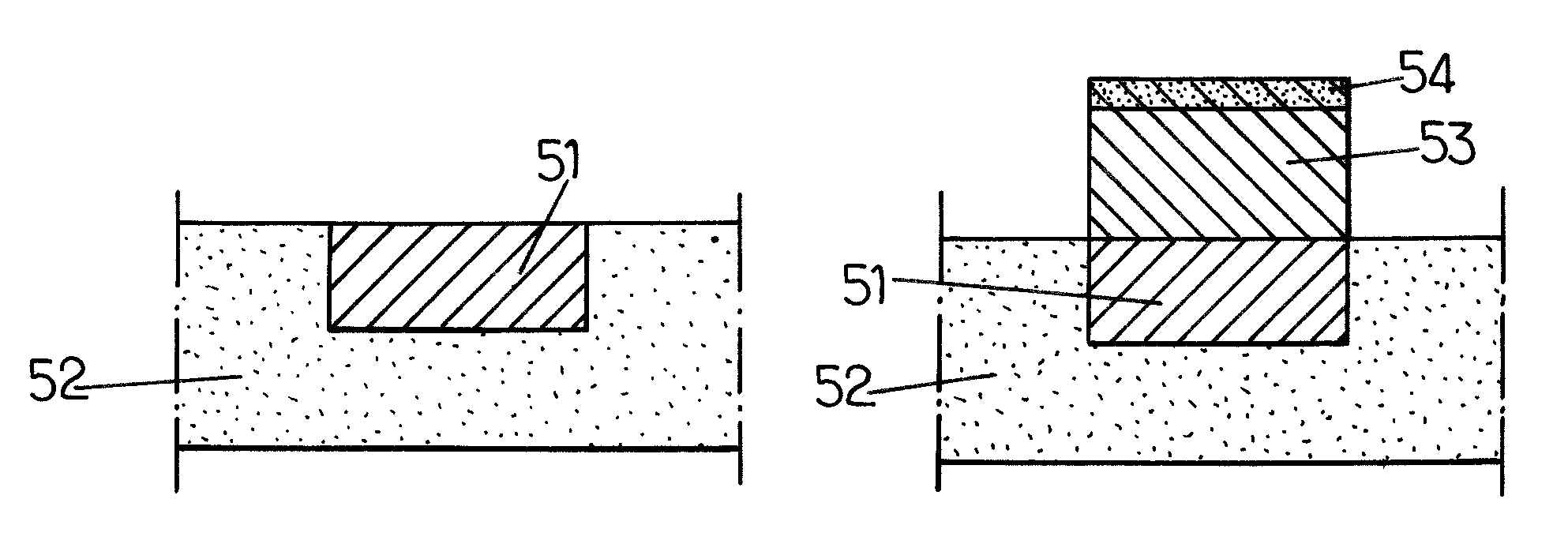
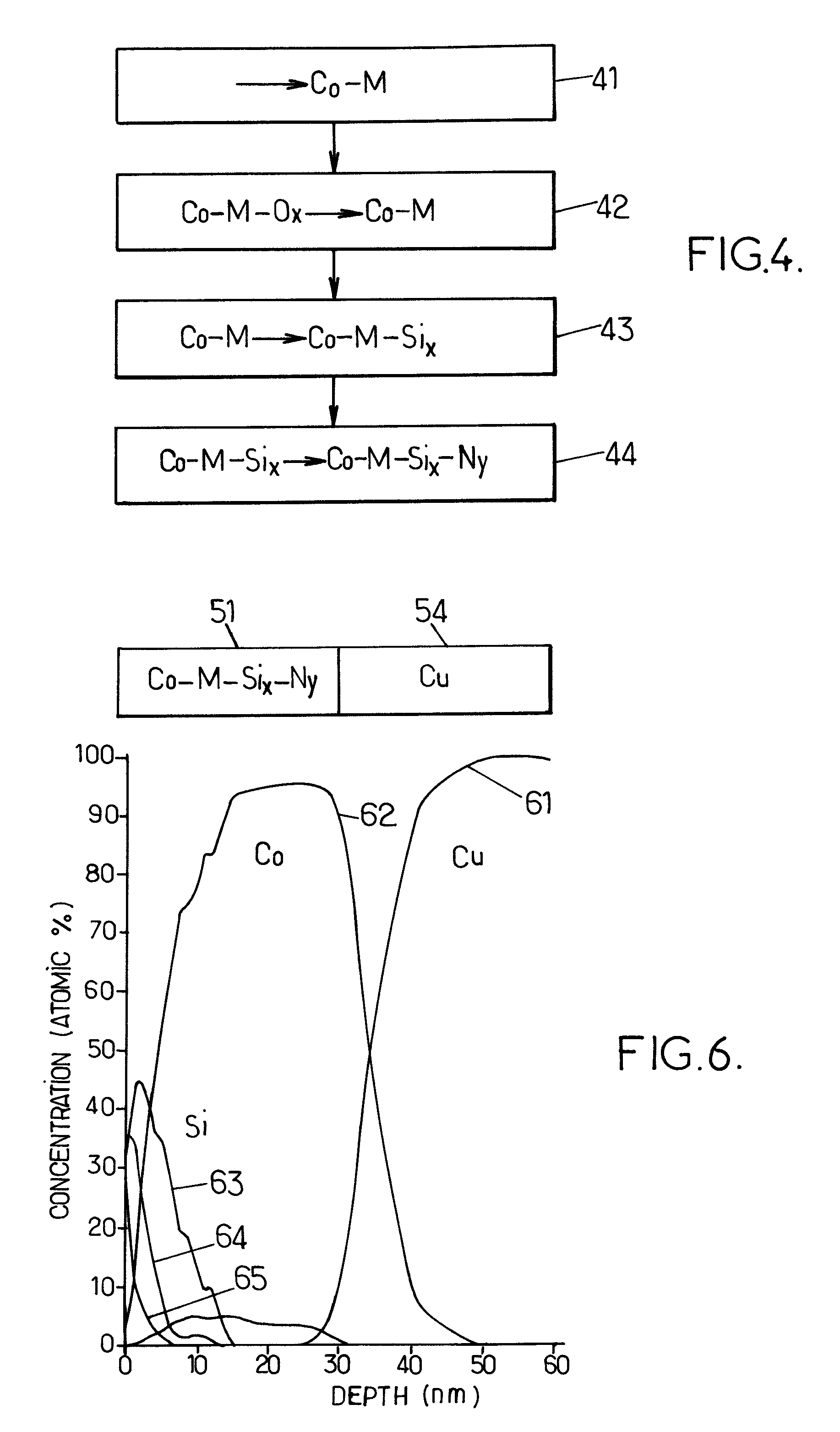
[0083]Metal barriers 98 with two layers of copper silicide obtained according to embodiments of the invention are situated between the copper portions constituted by the conductive paths 96 and the dielectric material of the interconnect structure 105. It is advantageous for these metal barriers 108 to be deposited in a self-aligned manner on the copper portions only.

[0084]In this example, the vias come into elect...


PUM

PropertyMeasurementUnit
thicknessaaaaaaaaaa
thicknessaaaaaaaaaa
rector temperatureaaaaaaaaaa

Abstract

A metal barrier is realized on top of a metal portion of a semiconductor product, by forming a metal layer on the surface of the metal portion, with this metal layer comprising a cobalt-based metal material. Then, after an optional deoxidation step, a silicidation step and a nitridation step of the cobalt-based metal material of the metal layer are performed. The antidiffusion properties of copper atoms (for example) and the antioxidation properties of the metal barrier are improved.

Description

PRIORITY CLAIM[0001]The present application is a translation of and claims priority from French Patent Application No. 06 09038 of the same title filed Oct. 13, 2006, the disclosure of which is hereby incorporated by reference to the maximum extent allowable by law.BACKGROUND OF THE INVENTION[0002]1. Technical Field of the Invention[0003]The present invention relates to the implementation of metal barriers in integrated electronic circuits.[0004]2. Description of Related Art[0005]Integrated circuits generally comprise such metal barriers at the interface between a conductive zone (typically a metal line or via in a multilayered interconnect structure) and an insulating zone (typically a dielectric layer in such a structure). These barriers prevent the diffusion of atoms from the conductive zone to the insulating zone, which can be the origin of integrated circuit malfunctions such as short-circuits between metal lines. This is why these barriers are commonly called “metal caps.”[000...

Claims


Application Information

Patent Timeline
Patent Type & Authority Patents(United States)
IPC IPC(8): H01L21/4763
CPCH01L21/76841H01L21/76849H01L23/53238H01L23/5226H01L21/76856H01L2924/0002H01L2924/00
Inventor DUMAS, LAURINJENNY, CECILECAUBET, PIERRE
Owner STMICROELECTRONICS SRL
Why Eureka
Try Eureka