SOI bottom pre-doping merged e-SiGe for poly height reduction

a technology of esige and polysilicate, which is applied in the field of soi bottom predoping merged esige for poly height reduction, can solve the problems of introducing other problems, affecting the operation of the transistor, and the gate is too short, so as to achieve the effect of reducing or even avoiding boron penetration of the transistor channel, sufficient boron ions, and superior operating characteristics

Inactive Publication Date: 2009-10-20
KK TOSHIBA
View PDF12 Cites 4 Cited by
  • Summary
  • Abstract
  • Description
  • Claims
  • Application Information

AI Technical Summary

Benefits of technology

[0006]Aspects of the present invention are directed to methods for manufacturing a semiconductor device, such as on a silicon-on-insulator (SOI) wafer, that has a transistor with source / drain regions that are sufficiently doped with boron ions while reducing or even avoiding boron penetration of the transistor channel. This may result in a transistor having superior operating characteristics such as a lower junction capacitance. Such a device may be provided without needing to manufacture excessively tall transistor gates, which may result in the transistor further having low parasitic capacitance, while utilizing a relatively simple and inexpensive set of manufacturing steps. In addition to achieving the above, the manufacturing process may further allow for the addition of a silicon germanium (SiGe) layer that provides compressive stress on the transistor channel, thereby improving hole mobility within the P-type transistor channel.

Problems solved by technology

For example, making the gate too tall can cause problems such as undesirable parasitic capacitance in the final product, as well as implant shadowing problems (especially where gates are repeated at a small scaled pitch) and difficulties in polysilicon etching during manufacturing.
On the other hand, making the gate too short can introduce other problems.
For example, during transistor manufacture, there is a trade-off between either allowing for undesirable boron penetration into the transistor channel or insufficiently doping the source / drain regions of the transistor.
While successfully avoiding channel boron penetration, the side effect of such a low energy dose is that source / drain region 3 is not fully doped such that it abuts BOX layer 4.
This can lead to an undesirably high junction capacitance.
Such channel boron penetration results in extensive degradation of channel mobility, which is quite undesirable.

Method used


Image

  • SOI bottom pre-doping merged e-SiGe for poly height reduction
  • SOI bottom pre-doping merged e-SiGe for poly height reduction
  • SOI bottom pre-doping merged e-SiGe for poly height reduction

Examples


Embodiment Construction

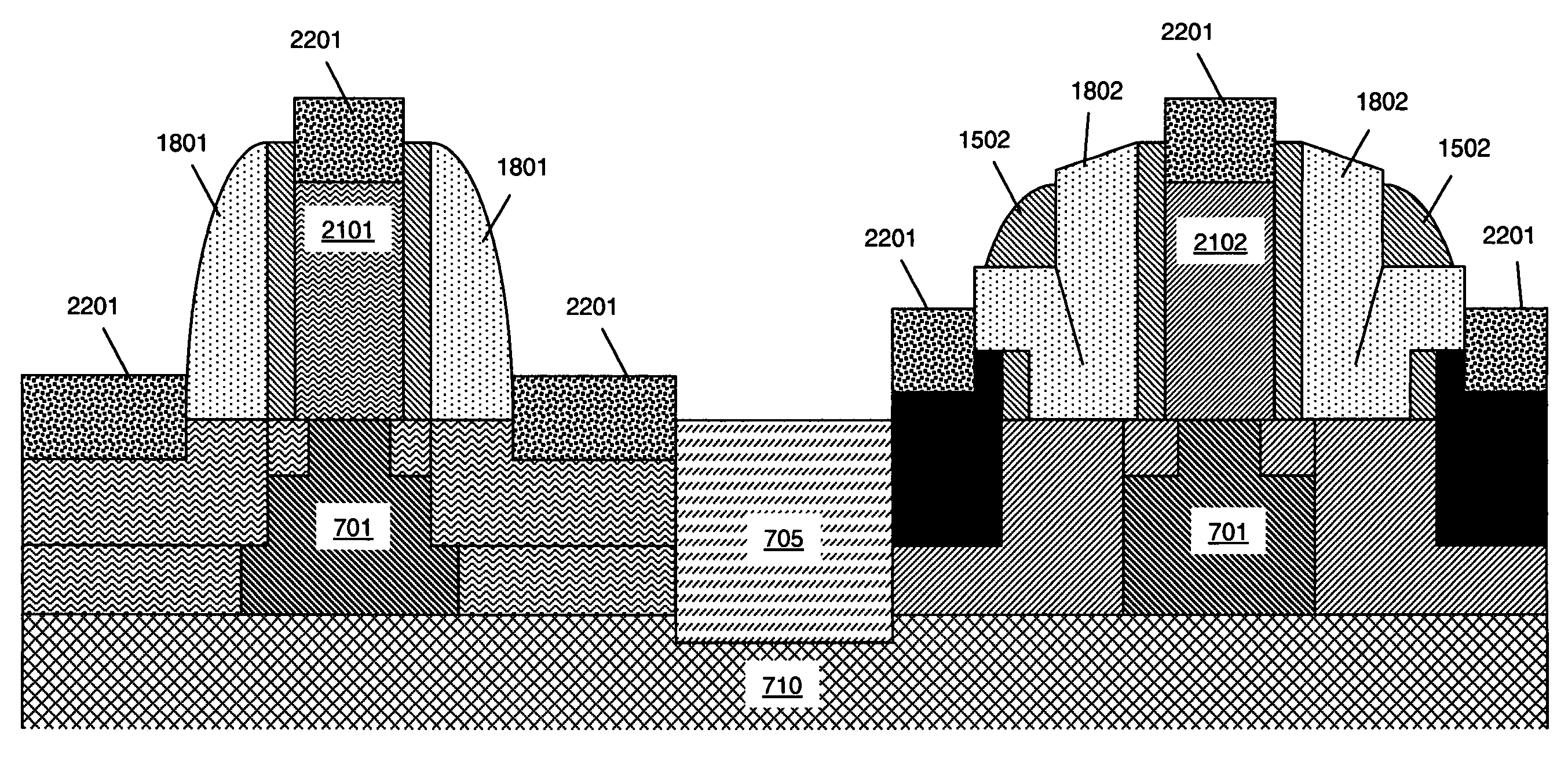
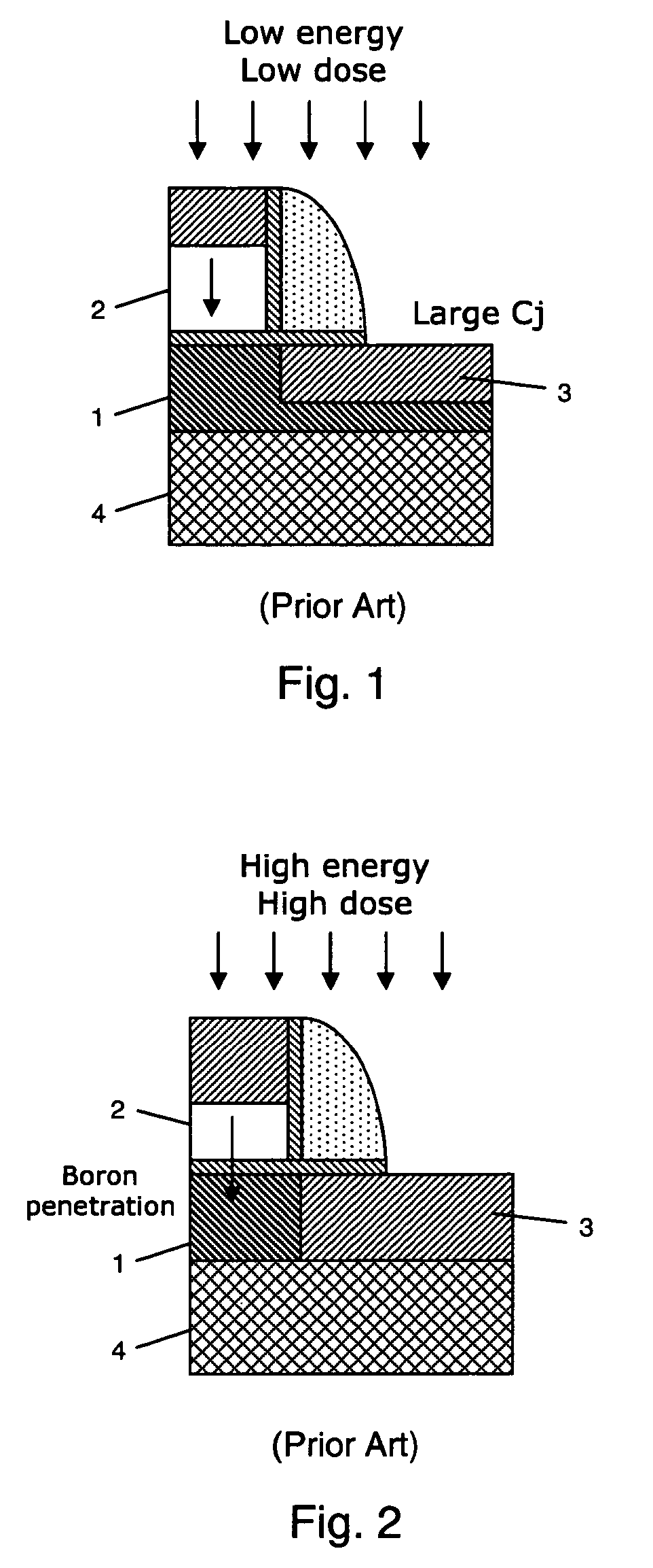
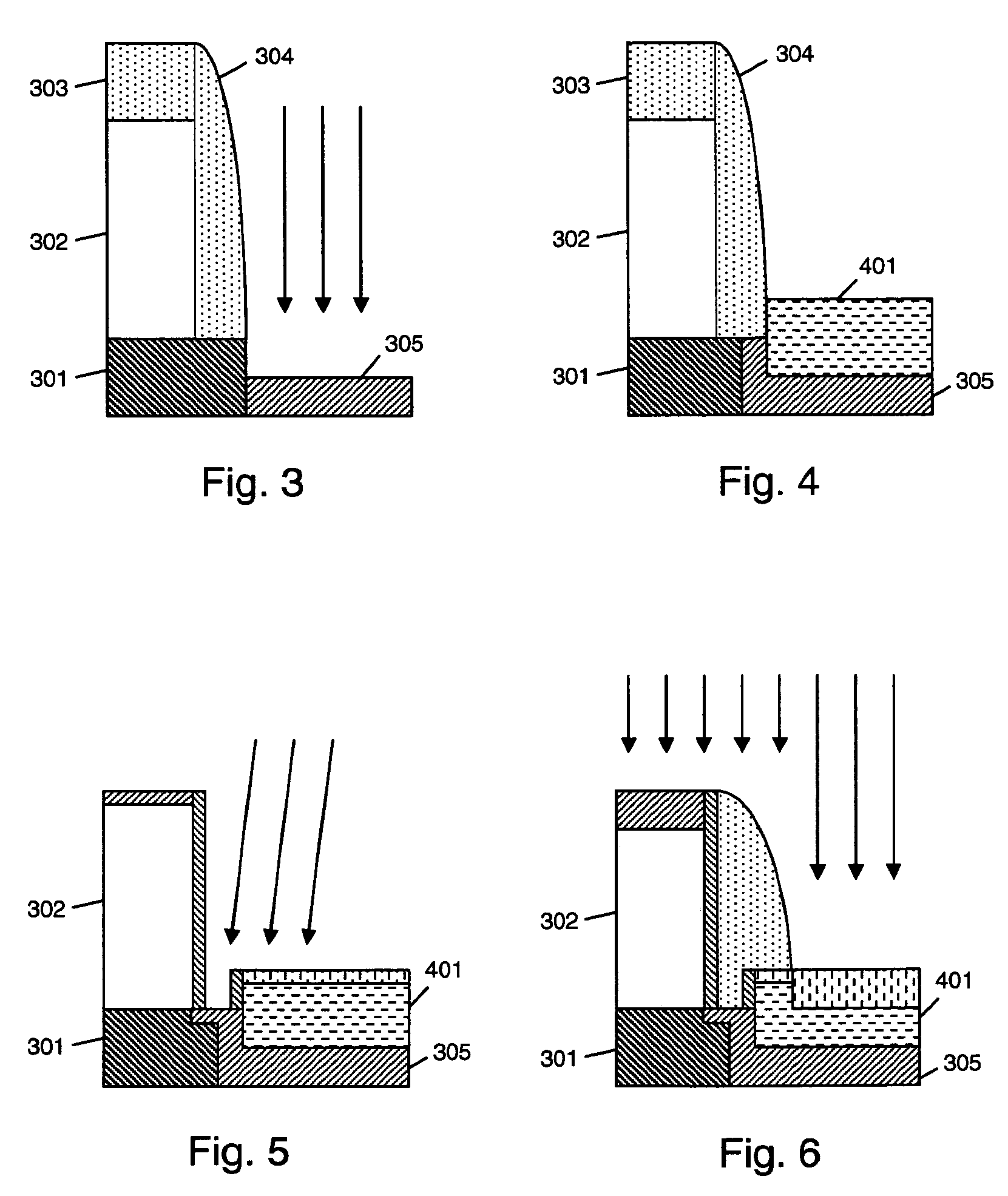
[0015]A summary highlighting certain steps in an illustrative manufacturing process will now be described in connection with FIGS. 3-6, which are presented in consecutive order as may be performed in the illustrative process. Referring to FIG. 3, a portion of a conventional SOI wafer is shown including a silicon body 301. A p-type field-effect transistor (PFET) polysilicon gate 302 is formed on silicon body 301, and sidewall spacers 304 are formed on the sidewalls of gate 302. Gate 302 is also capped with a SiN layer 303. A recessed portion 305 of silicon body 301 is pre-doped by boron implantation. Next, in FIG. 4, an SiGe layer 401 is epitaxially grown on recessed portion 305. After extension formation is performed in FIG. 5, then in FIG. 6 gate 302 and source / drain regions are implanted with low energy boron, thereby reducing or even avoiding boron penetration into the channel below gate 302. Such low energy boron may have an energy in the range of, for example, 2-10 KeV, such as...


PUM


Abstract

Semiconductor device structures, and methods for making such structures, are described that provide for fully-doped transistor source / drain regions while reducing or even avoiding boron penetration into the transistor channel, thereby improving the performance of the transistor. In addition, such a transistor may benefit from an SiGe layer that applies compressive stress to the transistor channel, thereby further improving the performance of the transistor.

Description

FIELD OF THE INVENTION[0001]Aspects of the present invention are generally directed to semiconductor devices and their methods for manufacture, and more particularly to providing a way to dope the source / drain regions of a transistor while reducing boron penetration into the transistor channel, and also to providing a SiGe layer in the same transistor that applies compressive stress to the transistor channel.BACKGROUND OF THE INVENTION[0002]Various types of silicon transistors often include a polysilicon gate. There are many factors that can influence the proper height of the gate. For example, making the gate too tall can cause problems such as undesirable parasitic capacitance in the final product, as well as implant shadowing problems (especially where gates are repeated at a small scaled pitch) and difficulties in polysilicon etching during manufacturing. Thus, it is desirable to limit the height of the polysilicon gate.[0003]On the other hand, making the gate too short can intr...

Claims


Application Information

Patent Timeline
Patent Type & Authority Patents(United States)
IPC IPC(8): H01L21/336
CPCH01L21/26586H01L29/8126H01L21/823814H01L21/84H01L27/1203H01L29/165H01L29/42316H01L29/6653H01L29/6656H01L29/6659H01L29/66628H01L29/66636H01L29/7834H01L29/7848H01L21/823807
Inventor KOHYAMA, YUSUKE
Owner KK TOSHIBA
Why Eureka
Try Eureka