
Driving method and circuit for automatic voltage output of active matrix organic light emitting device and data drive circuit using the same

a technology of organic light emitting devices and driving methods, which is applied in the direction of electric variable regulation, process and machine control, instruments, etc., can solve the problems of non-uniformity of brightness, the inability of induced voltages to be used as brightness information of pixels,

Inactive Publication Date: 2009-10-20
IKAIST CO LTD
View PDF5 Cites 43 Cited by
  • Summary
  • Abstract
  • Description
  • Claims
  • Application Information

AI Technical Summary

Benefits of technology

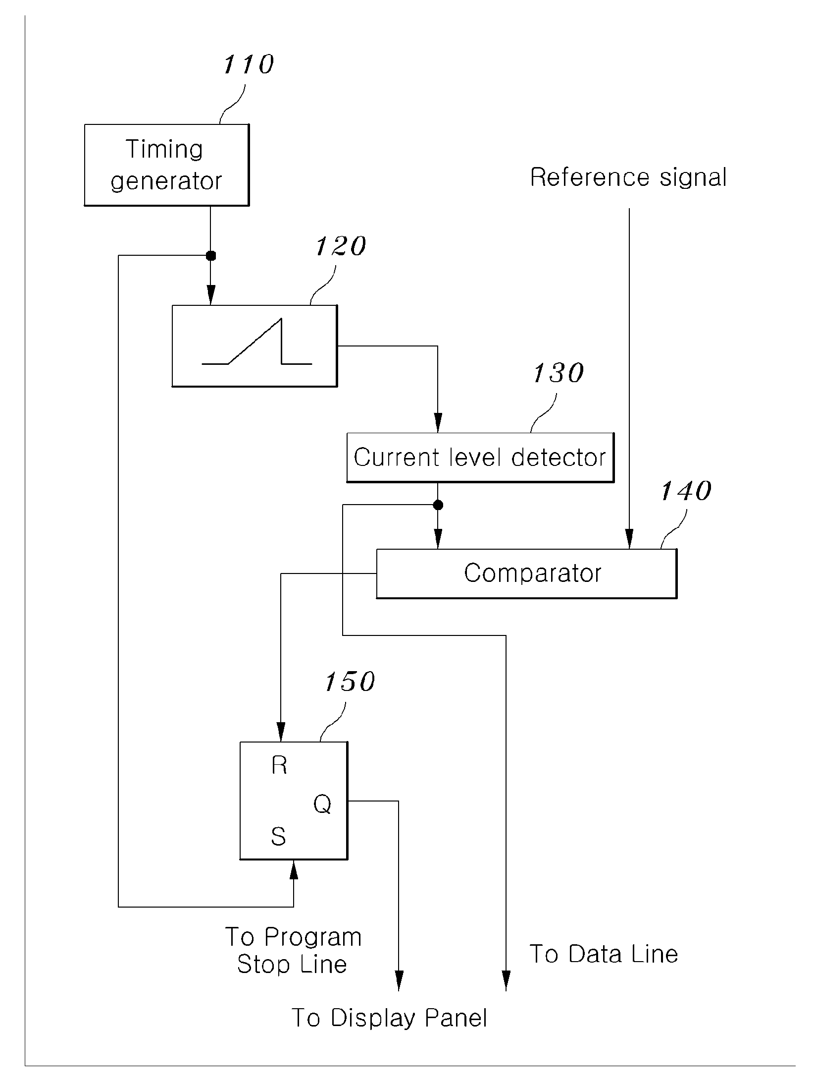
"The present invention provides a driving method and circuit for an active matrix organic light emitting device that monitors the amount of current applied to each pixel through a data line and adjusts the control signal to stop a data program when the current reaches a target value, to achieve uniform brightness between pixels. The invention also uses a voltage source as a data drive signal source to increase data drive speed and enhance the current drive capability of the voltage source. The driving circuit includes timing generation means, sweep voltage generation means, current level detection means, comparison means, and data writing start / end control signal generation means. The reference signals can be current or voltage signals, and the current drive levels of pixels are set to the reference current or voltage signal levels. The invention ensures that the current drive levels of pixels are controlled to be equal even though the voltage-current characteristics of transistors driving the OLEDs of the pixels are different."

Problems solved by technology

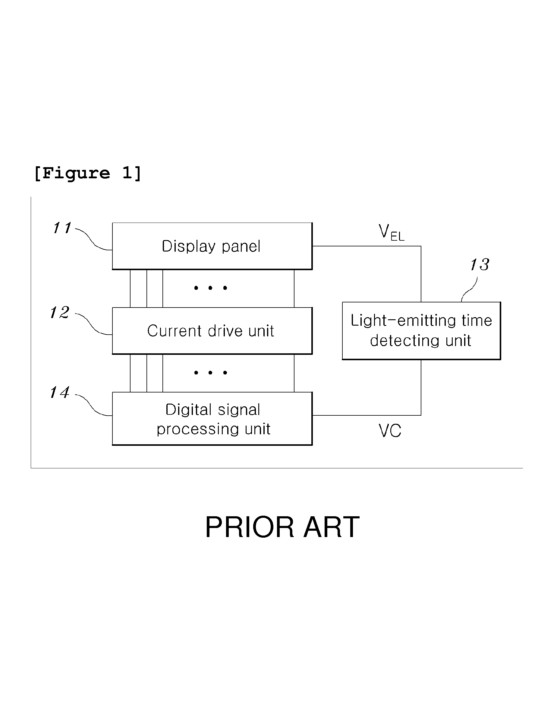
Furthermore, it is impossible that the induced voltages are used as the brightness information of the pixels unless they are used upon digital driving.
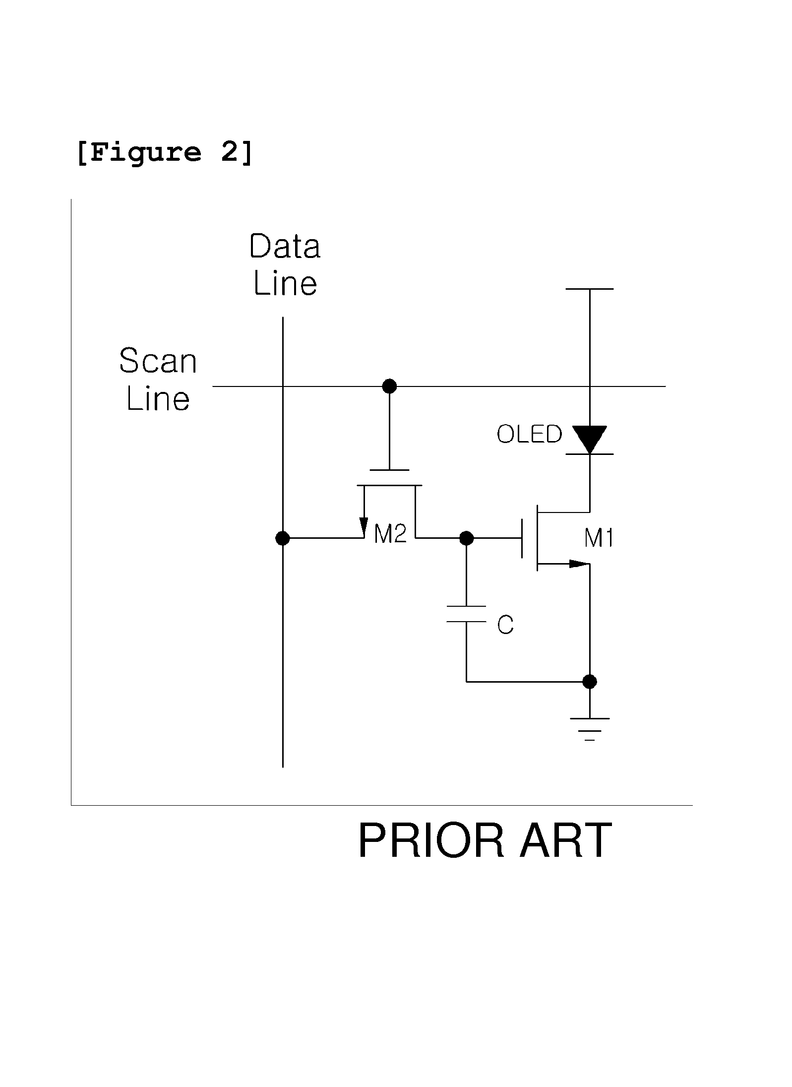
That is, a principal cause of the non-uniformity of brightness (such as panel-to-panel non-uniformity, and pixel-to-pixel non-uniformity in a panel) in a flat panel display using AMOLEDs is that the drive transistors of respective pixels, constituting the flat panel display, have different characteristics depending on pixels and the characteristics randomly vary over time.

Method used


Image

  • Driving method and circuit for automatic voltage output of active matrix organic light emitting device and data drive circuit using the same
  • Driving method and circuit for automatic voltage output of active matrix organic light emitting device and data drive circuit using the same
  • Driving method and circuit for automatic voltage output of active matrix organic light emitting device and data drive circuit using the same

Examples


Embodiment Construction

[0040]Reference now should be made to the drawings, in which the same reference numerals are used throughout the different drawings to designate the same or similar components.

[0041]FIG. 3 is a diagram illustrating the conceptual construction of a driving circuit for the automatic voltage output of an active matrix organic light emitting device according to the present invention.

[0042]As illustrated in FIG. 3, the drive circuit includes a timing generator 110 for generating a data drive start signal, a sweep voltage generator 120 for generating a sweep voltage signal in response to the output of the timing generator 110, a current level detector 130 for sensing the amount of current, which flows into pixels, based on the output of the sweep voltage generator 120 and outputting a sensing result to a data line, a comparator 140 for comparing the output of the current level detector 130 with a reference signal which determines the stop timing for data writing and outputting a correspon...


PUM


Abstract

Disclosed herein is a driving method and circuit for the automatic voltage output of an active matrix organic light emitting device, which is capable of resolving the non-uniformity of brightness between pixels. The circuit of the present invention includes timing generation means for generating a data drive start signal; sweep voltage generation means for generating a sweep voltage signal in response to output of the timing generation means; current level detection means for sensing an amount of current, which flows into pixels, based on output of the sweep voltage generation means, and outputting a sensing result to a data line; comparison means for comparing output of the current level detection means with a reference signal that determines stop timing for data writing, and outputting a comparison result; and data writing start / end control signal generation means for starting to operate in response to the output of the timing generation means, and generating data writing start and end control signals to a program stop line of a display panel. The invention can shorten data writing time and improve the precision of data writing. Furthermore, the present invention can simplify a data drive circuit and achieve the uniformity of brightness between pixels.

Description

BACKGROUND OF THE INVENTION[0001]1. Field of the Invention[0002]The present invention relates generally to a driving circuit for a flat panel display device and, more particularly, to a driving method and circuit for the automatic voltage output of an active matrix organic light emitting device, which is capable of resolving the non-uniformity of brightness between pixels, that is, a great problem in a flat panel display using the active-matrix organic light emitting device, and a data drive circuit using the same.[0003]2. Description of the Related Art[0004]Technologies for forming a Thin Film Transistor (TFT) on a substrate have been widely developed for the past several years, and applications of the technologies to an active-matrix display device are being developed.[0005]Particularly, since a TFT using a poly-silicon film has field-effect mobility higher than that of a conventional TFT using an amorphous silicon film, the TFT using the poly-silicon film can operate at a high sp...

Claims


Application Information

Patent Timeline
Patent Type & Authority Patents(United States)
IPC IPC(8): G09G3/36
CPCG09G3/3233G09G3/2014G09G2310/066G09G2300/0857G09G3/30
Inventor SON, YOUNG-SUKKIM, SANG-KYUNGCHO, GYU-HYEONG
Owner IKAIST CO LTD
Learn More