Laminated microfluidic structures and method for making

a microfluidic structure and polymer technology, applied in the field of microfluidics, can solve the problems of affecting the quality of the inorganic surface, and affecting the quality of the inorganic surface, and altering the mated surfa

Active Publication Date: 2009-10-27
RHEONIX INC
View PDF24 Cites 30 Cited by
  • Summary
  • Abstract
  • Description
  • Claims
  • Application Information

AI Technical Summary

Problems solved by technology

However, the material and production costs of the inorganic chips may become prohibitively high especially when the fluidic pathway(s) requires significant area or the chip has to be disposable.
The research effort required to redevelop these assays on inorganic surfaces would require significant time and resource investments.
However, the fabrication of polymeric microfluidic chips presents a variety of challenges.
Unfortunately, these techniques often significantly alter the mated surfaces and yield distorted or completely blocked microfluidic pathways due, for example, to the low dimensional rigidity of polymeric materials under the aforementioned bonding conditions.
However, the introduction of an adhesive layer to a wall surface of an enclosed fluid pathway can cause other fabrication and / or application problems.
The compressive force required to produce a uniform seal between component layers will often extrude the adhesive into the fluid pathways resulting in microchannel dimensional alteration or obstruction.
An additional potential problem with using adhesives is the formation of an adhesive wall within the enclosed microstructure.
The presence of this dissimilar material makes uniform surface modification of the microstructure difficult.
Furthermore, the manipulation or patterning of an adhesive layer is difficult, limiting the use of the adhesives to uniform continuous sheets or layers between two opposing planer surfaces.
This restricts fluidic communication through a network to one planer surface, as the fluid cannot flow through the adhesive layer, preventing the use of a more versatile three-dimensional space.
The use of the aforementioned strong solvents for bonding microfluidic chips with substrates composed of polystyrene, polycarbonate or acrylic is problematic.
That is, these solvents tend to over-soften or dissolve the surface of the substrates during the bonding process.
This may damage the microfluidic structure by completely erasing, blocking or destroying the fluid pathways when the substrates are laminated.
Although it is possible to weaken the solvent strength by mixing the solvent with “inert” solvents such as methanol or ethanol, the resulting bond often does not provide a satisfactory result.
It is apparent, however, that these approaches rely on stringent control of the fabrication and process conditions, which may result in unacceptable fabrication throughput and production yield.
Consequently, its application to microfluidic chip manufacturing is restricted.
The significant challenge of dispensing the correct volume of bonding material into the relief structures is not addressed.
The necessary control of the small volume of bonding material does not lend itself to high production yields.

Method used


Image

  • Laminated microfluidic structures and method for making
  • Laminated microfluidic structures and method for making
  • Laminated microfluidic structures and method for making

Examples


Embodiment Construction

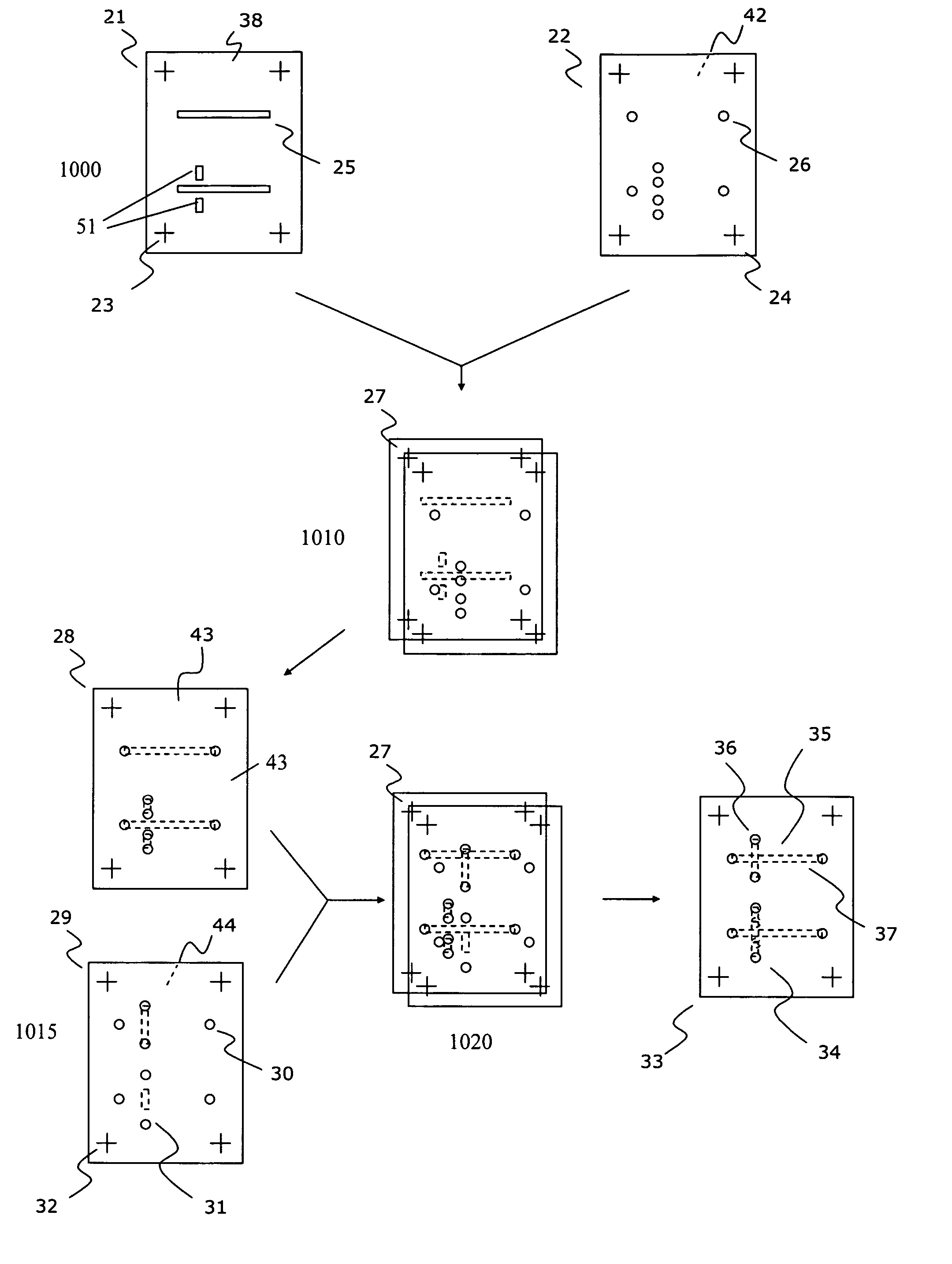
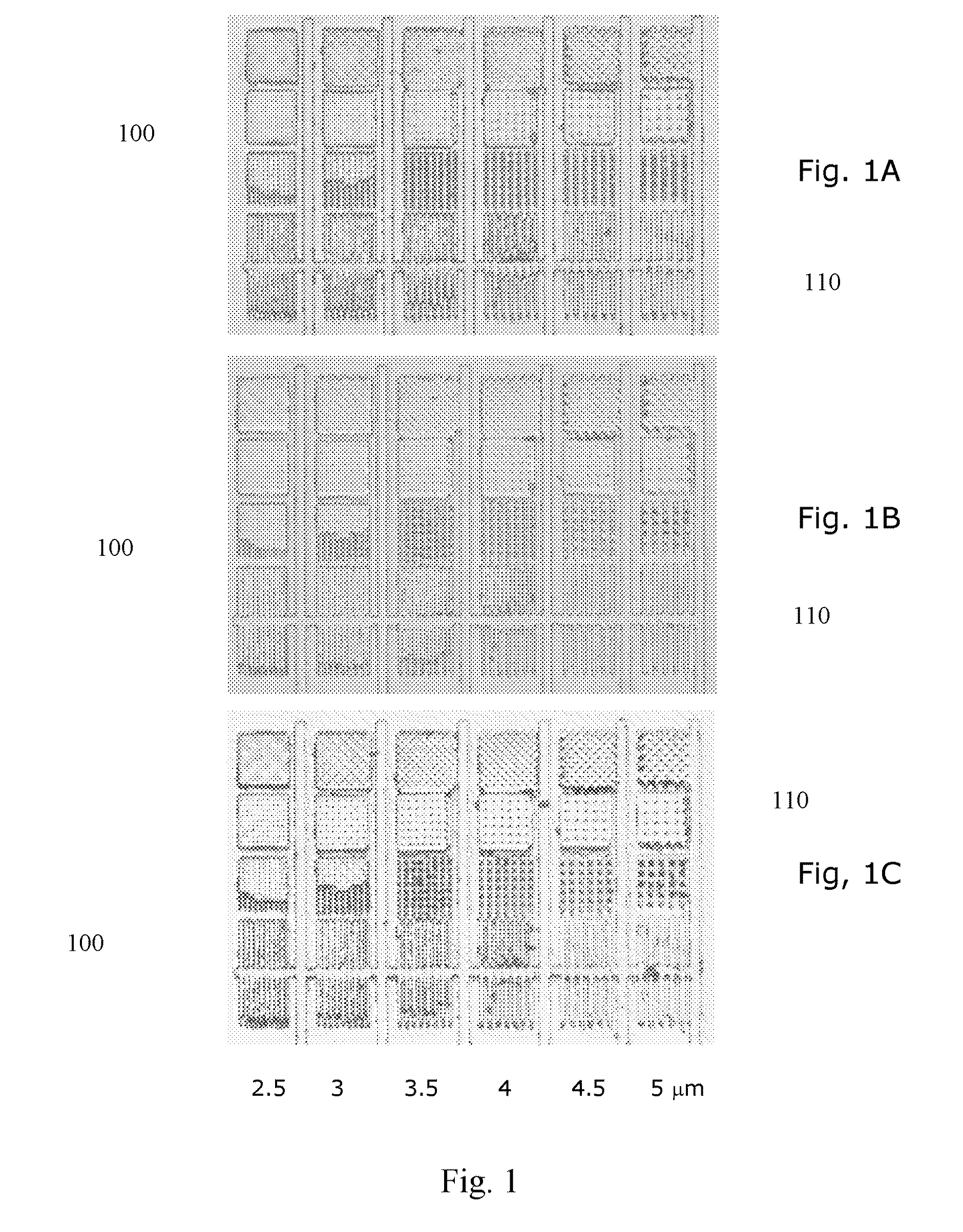
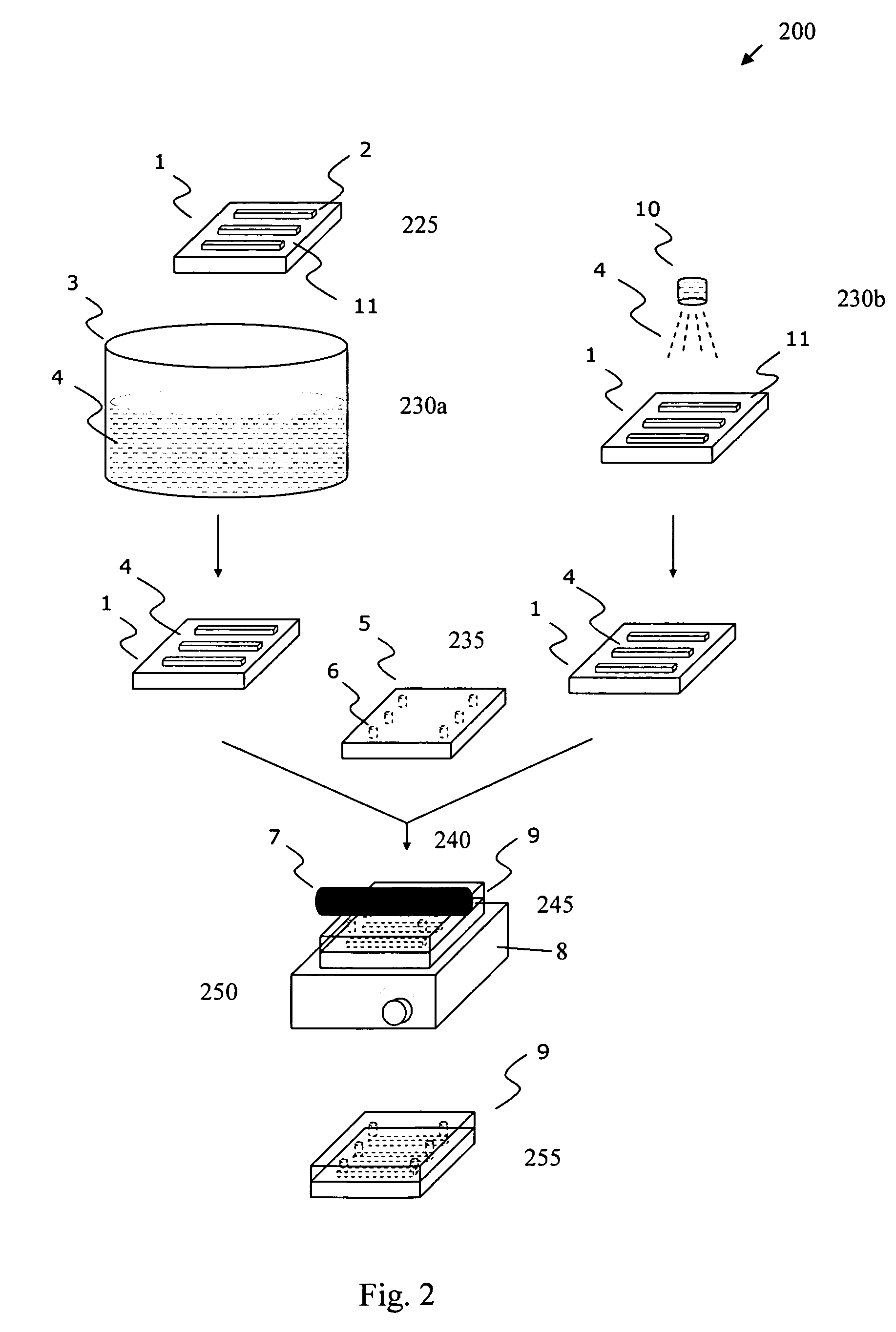
[0027]As used herein, the word “microstructure” generally refers to structural features on a microfluidic substrate component with walls having at least one dimension in the range of about 0.1 micrometer to about 1000 micrometers. These features may be, but are not limited to, microchannels, microfluidic pathways, microreservoirs, microvalves or microfilters. The term “polymeric” refers to a macromolecular structure or material having a molecular weight that is substantially higher than the constituent monomers and, which is produced by a polymerization reaction. All materials commonly and herein referred to as “plastic” materials are polymeric materials. The term “acrylic” refers to Acrylite®, Plexiglas®, PMMA or other trade names of polymethylmethacrylate. A “two-dimensional microfluidic network” refers to fluidic connectivity of at least two microfluidic pathways or channels that co-exist within a component or in the plane of a planar component. A “three-dimensional microfluidic ...


PUM

PropertyMeasurementUnit
thicknessesaaaaaaaaaa
temperatureaaaaaaaaaa

Abstract

A method for making a polymeric microfluidic structure in which two or more components (layers) of the microfluidic structure are fixedly bonded or laminated with a weak solvent bonding agent, particularly acetonitrile or a mixture of acetonitrile and alcohol. In an aspect, acetonitrile can be used as a weak solvent bonding agent to enclose a microstructure fabricated in or on a non-elastomeric polymer such as polystyrene, polycarbonate, acrylic or other linear polymer to form a three-dimensional microfluidic network. The method involves the steps of wetting at least one of the opposing surfaces of the polymeric substrate components with the weak solvent bonding agent in a given, lower temperature range, adjacently contacting the opposing surfaces, and thermally activating the bonding agent at a higher temperature than the lower temperature range for a given period of time. The contacted polymeric substrates may also be aligned prior to thermal activation and compressed during thermal activation. A laminated, polymeric microfluidic structure is also disclosed.

Description

BACKGROUND OF THE INVENTION[0001]1. Field of the Invention[0002]Embodiments of the invention generally pertain to the field of microfluidics and, more particularly, to a laminated, polymeric microfluidic structure and to a method for making a laminated, polymeric microfluidic structure.[0003]2. Description of Related Art[0004]The technology of manipulating minute volumes of biological and chemical fluids is widely referred to as microfluidics. The realized and potential applications of microfluidics include disease diagnosis, life science research, biological and / or chemical sensor development, and others appreciated by those skilled in the art.[0005]A microfluidic structure including a substrate having one or more microfluidic channels or pathways and a cover plate or a second or more substrates with fluid pathways that may or may not be interconnected, may commonly be referred to as a microfluidic chip. Highly integrated microfluidic chips are sometimes called ‘labs on a chip’. In...

Claims


Application Information

Patent Timeline
Patent Type & Authority Patents(United States)
IPC IPC(8): B32B38/04
CPCB01F5/0683B01F11/0071B01F13/0059B01L3/502707B29C65/4895B29C66/54F04B43/043F04B43/06F16K99/0001F16K99/0015F16K99/0021F16K99/0055F16K99/0057B32B37/0038B29C66/543B01F5/0688Y10T156/1002B01L2200/12B01L2300/0816B01L2300/0861B01L2300/0867B01L2300/0887B01L2400/0481B01L2400/0655B01L2400/084B29L2031/756F16K99/0034F16K2099/0074F16K2099/0078F16K2099/0084F16K2099/0094B29C66/83411B29C66/8362B29C66/71B29C66/1122B01F25/451B01F25/4521B01F31/65B01F33/30B29K2069/00B29K2033/08B29K2025/06
Inventor ZHOU, PENGYOUNG, LINCOLN C.
Owner RHEONIX INC
Why Eureka
Try Eureka