Method of fabricating a chip

a technology of electronic chips and manufacturing methods, applied in the direction of coupling device connections, semiconductor/solid-state device testing/measurement, instruments, etc., can solve the problems of affecting the first electronic component, and the electronic device does not function as designed, etc., to reduce the cost of fabricating chips, increase manufacturing flexibility, and easy to change

Active Publication Date: 2009-10-27
KINGSTON DIGITAL CO LTD
View PDF15 Cites 4 Cited by
  • Summary
  • Abstract
  • Description
  • Claims
  • Application Information

AI Technical Summary

Benefits of technology

[0008]The method discussed herein in fabricating a chip addresses the problems identified above as well as other problems identified herein and those that are known in the art. In an aspect of the present invention, a chip is provided wherein a first electrical part is embedded in a shell, and a determination is made whether the first electrical part is defective or functional before a second electrical part is placed in communication with the first electrical part and committed thereto. If the first electrical part is determined to be defective, then the shell with the defective first electrical part may be rejected. Conversely, if the first electrical part or a test result of the first electrical part indicates that the first electrical part is functional or good then the second electrical part may be connected to the first electrical part. In this manner, second electrical parts are connected or committed only to functional first electrical parts thereby reducing or eliminating the possibility of wasting second electrical parts due to damaged first electrical parts.
[0015]The method of fabricating the chip discussed herein increases manufacturing flexibility because the type of chip fabricated may be easily changed by using different first and second electrical parts combination. For example, the chip fabricator may fabricate a plurality of shells with a first electrical part embedded in each shell. The first electrical part may be operative to control a plurality of different types of second electrical parts. A lead frame may also be embedded in the shell which provides electrical communication between the first electrical part and the second electrical part. The lead frame may also be electrically connectable to the plurality of different types of second electrical parts such as a 512 MB memory IC or a 1 GB memory IC. The chip fabricator may stock a bulk quantity of 512 MB memory IC and a bulk quantity of 1 GB memory IC. The chip fabricator may connect 512 MB memory IC or 1 GB memory IC to the first electrical part embedded in the shell when an order for such memory chips are received by the chip fabricator.
[0016]Additionally, the method of fabricating the chip discussed herein reduces the cost to fabricate chips because less first and second electrical parts are discarded. The reason is that first electrical parts are only committed to functional second electrical parts, and conversely, second electrical parts are only committed to functional first electrical parts.

Problems solved by technology

Unfortunately, during the process of attaching the first electronic component to the electronic board, situations may arise that may harm the first electronic component.
For example, the first electronic component may be soldered to the electronic board wherein the soldering process exposes the first electronic component to excessive heat thereby damaging the first electronic component.
However, at the end of the assembly process, the assembler may discover that the electronic device does not function as designed due to the damaged first electronic component.
The assembler must then begin to debug the electronic device to locate and repair the damaged first electronic component at great expense and time.
Likewise, the manufacturer of the electronic component may encounter a similar type of problem when manufacturing or fabricating the electronic component.
Unfortunately, the molding processes may harm the controller integrated circuit and / or the memory integrated circuit thereby preventing the memory card from functioning properly after molding.
Alternatively, if only one of the electrical parts was damaged by the molding process, both the defective and the non-defective electrical part must be discarded thereby wasting not only the defective electrical part but also the non-defective electrical part.
Nonetheless, when either one of the electrical parts become defective due to the molding process, then the repair technician must consume time and energy to remove the defective electrical part, to repair the electrical part or to salvage the non-defective electrical part.

Method used


Image

  • Method of fabricating a chip
  • Method of fabricating a chip
  • Method of fabricating a chip

Examples


Embodiment Construction

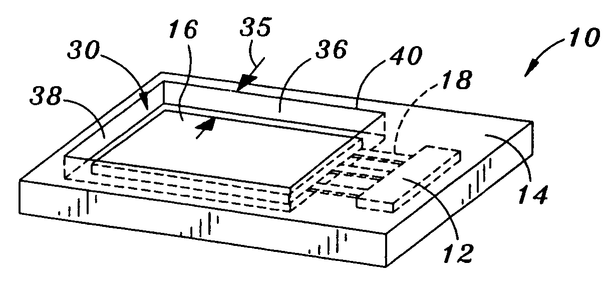
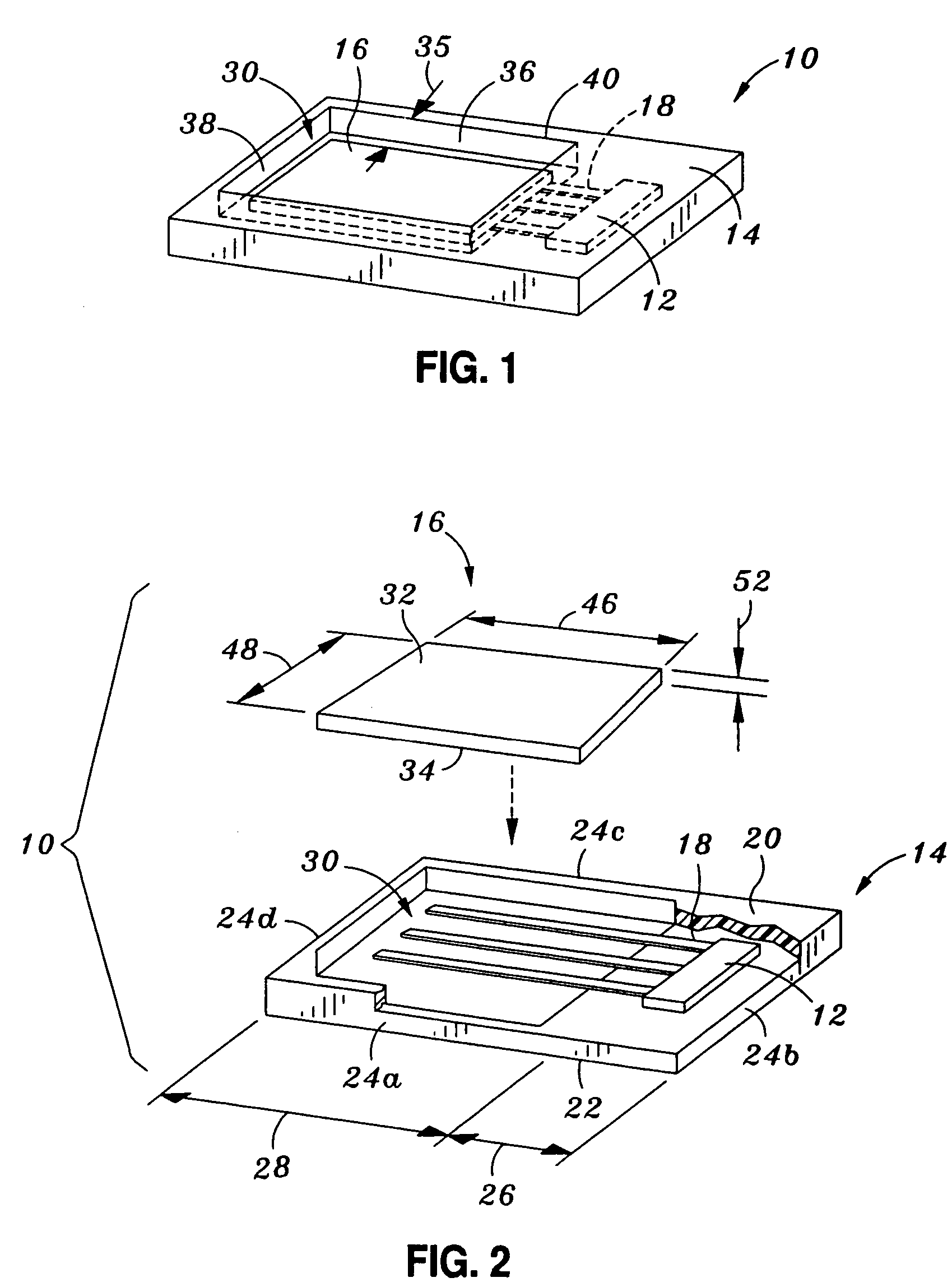
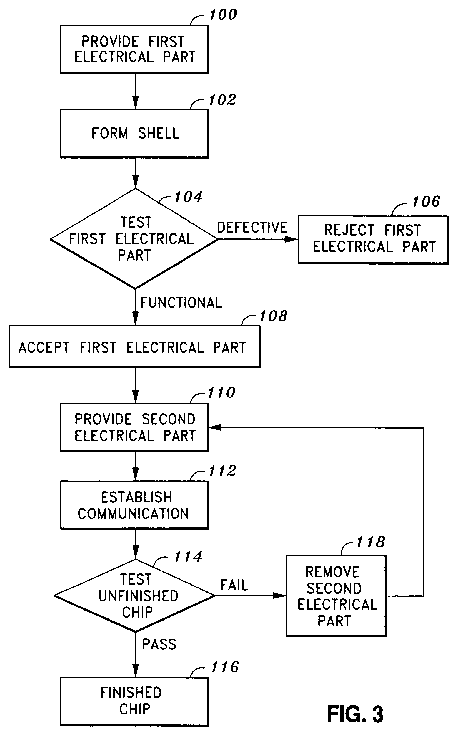
[0024]Referring now to FIG. 1, a chip 10 is shown wherein a first electrical part 12 is embedded in a shell 14 and it is determined whether the first electrical part 12 is defective or functional before a second electrical part 16 is placed in communication with the first electrical part12 and committed thereto. If the first electrical part 12 is determined to be defective, then the shell 14 with the defective first electrical part 12 is rejected. Conversely, if a test result of the first electrical part 12 indicates that the first electrical part 12 is functional or good then the second electrical part 16 is connected to the first electrical part 12. In this manner, second electrical parts 16 are connected or committed only to functional first electrical parts 12.

[0025]As will be discussed further herein, a method of fabricating the chip 10 and the structure of the chip 10 are disclosed. Although the chip 10 shown in FIG. 1 has two electrical parts, namely, first and second electri...


PUM


Abstract

A method of fabricating a chip may include the step of providing a first electrical part. The method may also include the step of forming a shell with the first electrical part embedded in a first side portion of the shell and a cavity in a second side portion of the shell. The method may include the step of testing the embedded first electrical part to determine whether the first electrical part is defective or functional. The method may also include the steps of providing a second electrical part, inserting the second electrical part within the cavity of the shell second side portion, establishing electrical communication between the first and second electrical parts if a test result of the first electrical part indicates that the first electrical part is functional, and finishing the chip. Also, the method may include the step of rejecting the first electrical part if the test result of the first electrical part indicates that the first electrical part is defective.

Description

CROSS-REFERENCE TO RELATED APPLICATIONS[0001]Not ApplicableSTATEMENT RE: FEDERALLY SPONSORED RESEARCH / DEVELOPMENT[0002]Not ApplicableBACKGROUND[0003]The present invention relates to a method of fabricating electronic chips, and more particularly, digital memory cards.[0004]Electronic devices (e.g., computer) may contain many different types of electronic components such as memory cards and processors to name a few which are assembled together to build the electronic device. In the assembly of the electronic device, these electronic components may be received by an assembler. The assembler may begin to assemble the electronic device by attaching a first electronic component to an electronic board. Unfortunately, during the process of attaching the first electronic component to the electronic board, situations may arise that may harm the first electronic component. For example, the first electronic component may be soldered to the electronic board wherein the soldering process exposes...

Claims


Application Information

Patent Timeline
Patent Type & Authority Patents(United States)
IPC IPC(8): H01L21/66
CPCG11C29/00H01L22/20H01L22/14H01L2924/014
Inventor KOH, WEI
Owner KINGSTON DIGITAL CO LTD
Why Eureka
Try Eureka