

Methods and apparatus for making placement sensitive logic modifications
a logic modification and logic technology, applied in the direction of error detection/correction, instruments, cad circuit design, etc., can solve the problems of large-scale modification of an existing chip design that can be exceptionally difficult, work using such a prior technique would generally have a negative impact on the design cycle, time to market, and design reuse, so as to shorten the design cycle and reduce risk. , the effect of reducing the design and development tim
- Summary
- Abstract
- Description
- Claims
- Application Information
AI Technical Summary
Benefits of technology
Problems solved by technology
Method used
Image

Examples
Embodiment Construction
[0023]The present invention will now be described more fully with reference to the accompanying drawings, in which several embodiments and various aspects of the invention are shown. This invention may, however, be embodied in various forms and should not be construed as being limited to the embodiments set forth herein. Rather, these embodiments are provided so that this disclosure will be thorough and complete, and will fully convey the scope of the invention to those skilled in the art.
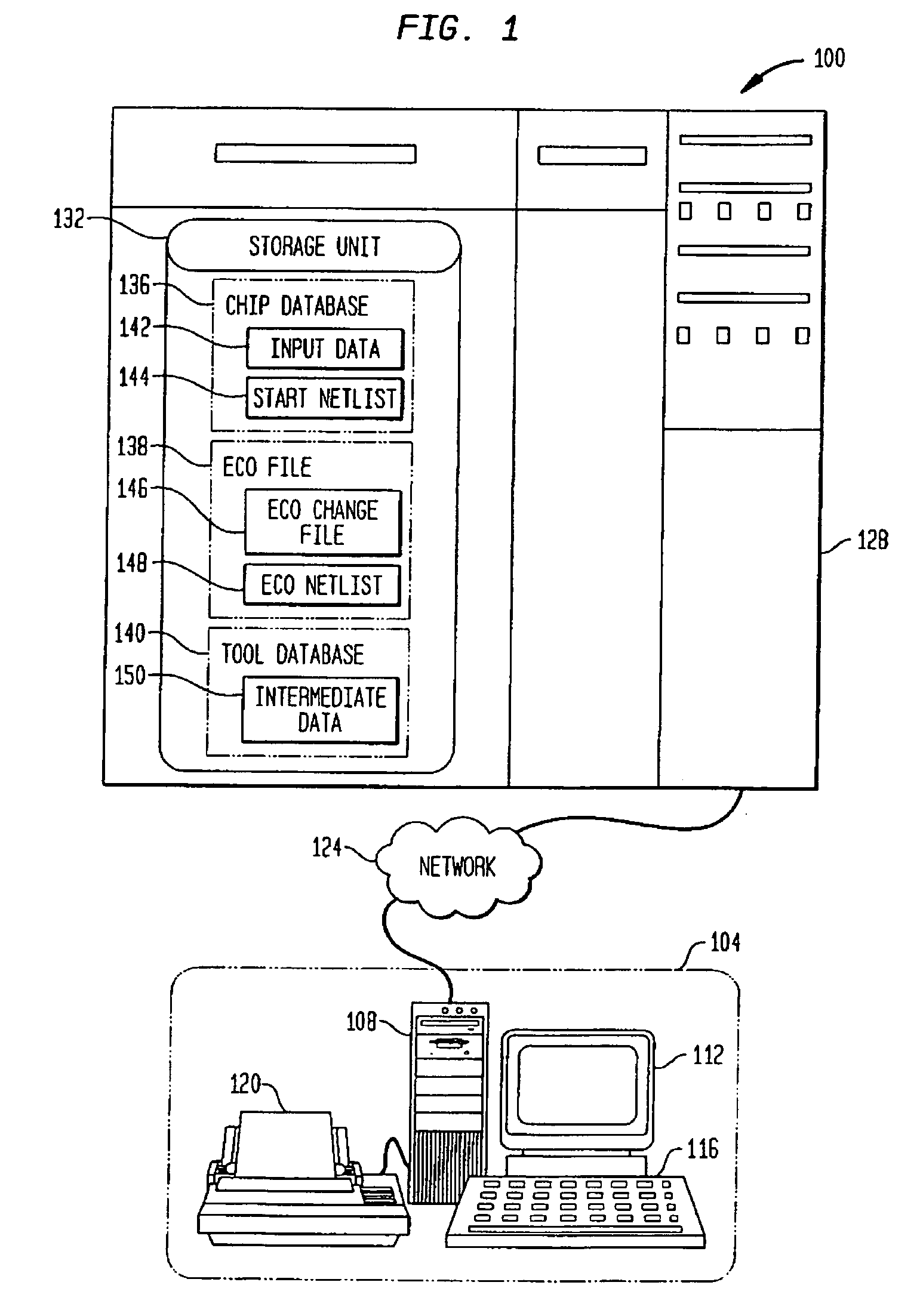
[0024]FIG. 1 illustrates an automated change design systems 100 in accordance with an embodiment of the present invention. The automated change design system 100 may suitably include a work station 104 consisting, for example, of a processor complex 108, a monitor 112, a keyboard / mouse 116, and may include a printer 120. The work station 104 is connected to a network 124. This connection may be made utilizing the Internet or a local intra-net, for example. The network 124 is then further connected ...
PUM
 Abstract
Description
Claims
Application Information