Electrophoresis device, method of driving electrophoresis device, and electronic apparatus

a technology of electrophoresis device and electrophoresis device, which is applied in the direction of electric digital data processing, instruments, computing, etc., can solve the problems of delay, further difficulty in obtaining reliability, and difficulty in obtaining tft reliability, so as to prevent image quality deterioration, increase reliability of display unit using electrophoresis device, and display switch

Active Publication Date: 2009-11-03
E INK CORPORATION
View PDF9 Cites 202 Cited by
  • Summary
  • Abstract
  • Description
  • Claims
  • Application Information

AI Technical Summary

Benefits of technology

[0026]Accordingly, the present invention is designed to solve the above-mentioned problems, and it is an object of the present invention to provide an electrophoresis device, a method of driving the electrophoresis device, and an electronic apparatus including the electrophoresis device, capable of preventing the deterioration of contrast and of improving image quality.

Problems solved by technology

However, the electrophoresis device formed by combining the electro phoretic ink constructed in the microcapsule manner and the active matrix type of element array has problems of a driving method as follows.
However, for the voltage applied to the pixel electrode, the driving voltage is too high when switching the TFT connected to the pixel electrode, so that it is difficult to obtain the reliability of the TFT.
In this case, it is further difficult to obtain reliability.
However, this method has the following problems.
However, since applying the voltage to each pixel electrode is performed by sequentially selecting each pixel transistor, the timing when applying the voltage to each pixel electrode does not coincide with the timing when applying the voltage to the common electrode, so that delay occurs.
As a result, there is a fear that the erroneous rewriting occurs.
In addition, even though the voltage is applied to each pixel electrode before the erroneous rewriting occurs, the voltage of the pixel electrode gradually decreases due to the leakage of the pixel transistor.
There is a possibility that the erroneous rewriting will occur.
However, the above-mentioned conventional display device (electrophoresis device) has the following problems.
However, since the switching element or wiring line is generally connected to the pixel electrode 1 (1a and 1b), the pixel electrode is subjected to a voltage drop due to the channel resistance or wiring resistance and the influence of the wiring capacity or the like.
As a result, the particles 3 and 4 move a little from the locations at the time when deleting the image and a gray color is displayed at the portions on which the white color, functioning as the background color, must be originally displayed, thereby deteriorating contrast and image quality.

Method used


Image

  • Electrophoresis device, method of driving electrophoresis device, and electronic apparatus
  • Electrophoresis device, method of driving electrophoresis device, and electronic apparatus
  • Electrophoresis device, method of driving electrophoresis device, and electronic apparatus

Examples


first embodiment

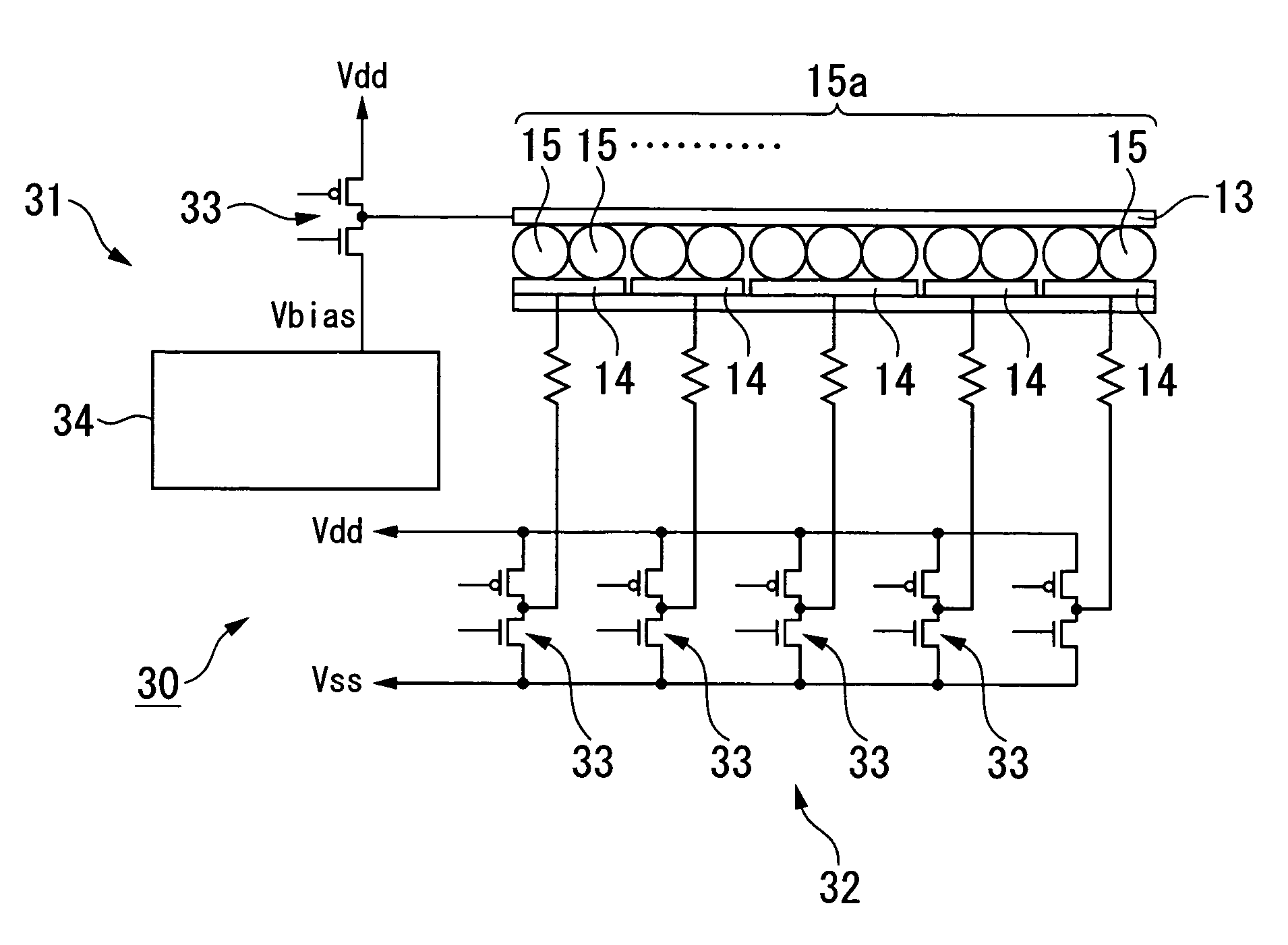
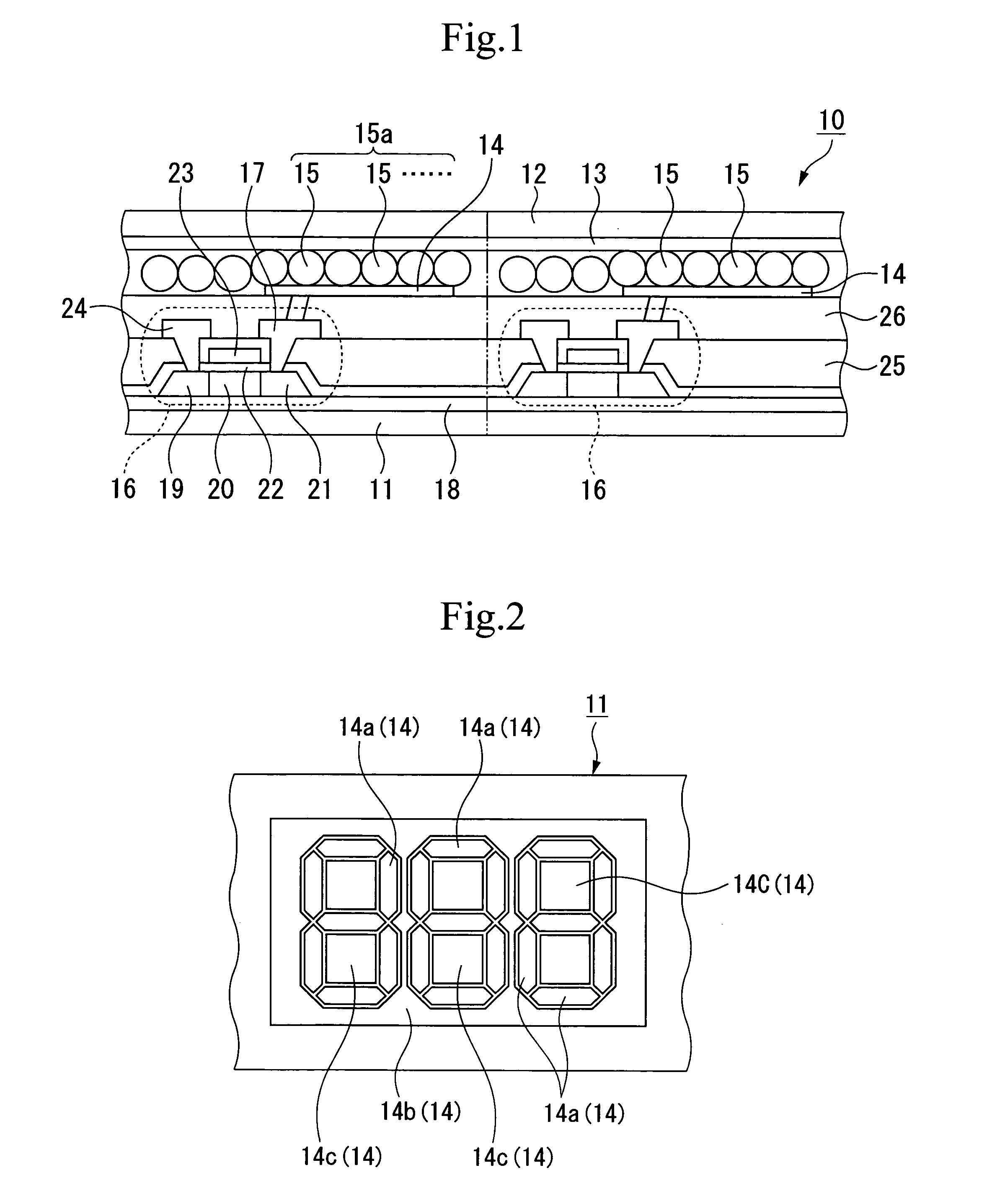
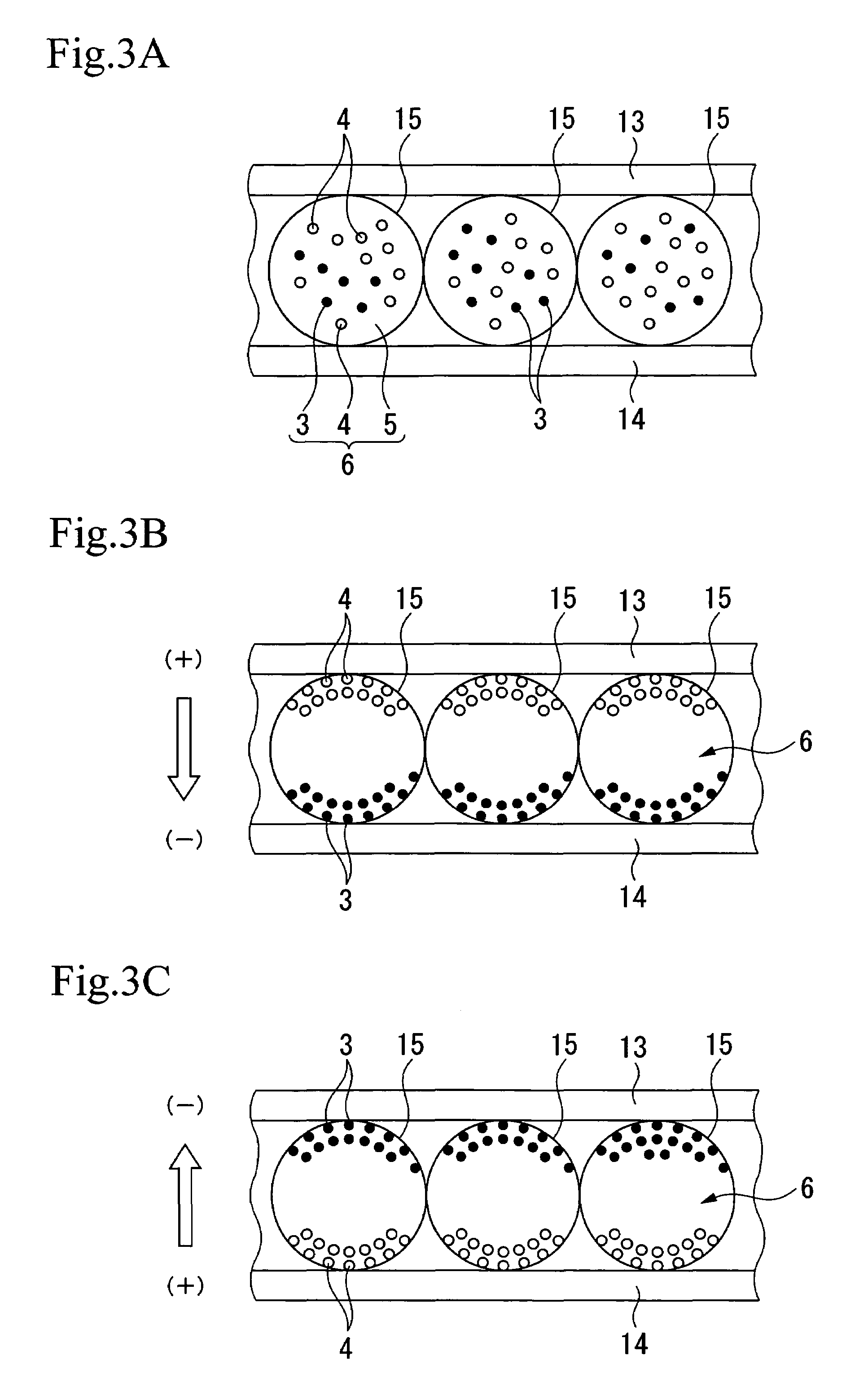
[0063]FIG. 1 shows an electrophoresis device according to a first embodiment of the present invention. In FIG. 1, reference numeral 10 indicates an electrophoresis device. The electrophoresis device 10 is formed by attaching a counter substrate 12 on a substrate 11. A common electrode 13 is provided at the inner side of the counter substrate 12, and a microcapsule layer 15a is provided between the common electrode 13 and pixel electrodes 14 formed on the substrate 11. The microcapsule layer 15a is composed of microcapsules 15 encapsulating electrophoresis particles therein.

[0064]A drain electrode 17 of a TFT (thin film transistor) 16 is connected in series to each pixel electrode 14, and the TFT 16 serves as a switching element.

[0065]In addition, in the electrophoresis device 10 having the above-mentioned structure, one of the substrate 11 and the counter substrate 12 serves as a display surface (an observation surface). In addition, the electrode and the substrate serving as the di...

second embodiment

[0112]Next, an electrophoresis device according to a second embodiment of present invention will be described.

[0113]The second embodiment of the present invention is mainly different from the first embodiment in that electrodes arranged in a dot shape are used as the pixel electrodes instead of using the segment electrodes corresponding to display image, and that the electrodes are driven in an active matrix manner.

[0114]FIG. 6 is a diagram showing an electrophoresis device according to a second embodiment of the present invention. In FIG. 6, reference numeral 40 indicates the electrophoresis device. The electrophoresis device 40 has a microcapsule layer 15a composed of the microcapsules 15 interposed between a substrate (not shown) including a plurality of pixel electrodes 41 and a substrate (not shown) including a common electrode.

[0115]On one substrate on which the pixel electrodes 41 are formed, a plurality of data lines 42, a plurality of scanning lines 43 intersecting the plur...

third embodiment

[0129]Next, an electrophoresis device according to a third embodiment of the present invention will be described.

[0130]The third embodiment of the present invention is mainly different from the second embodiment in that the electrophoresis device according to the third embodiment is an in-plane type.

[0131]FIGS. 7A and 7B are diagrams showing the electrophoresis device according to the third embodiment of the present invention. In FIGS. 7A and 7B, reference numeral 50 indicates an electrophoresis device. The electrophoresis device 50 is an in-plane type, and a plurality of pixel electrodes 52 and a plurality of common electrodes 53 are formed on one substrate 51 as shown in a side cross-sectional view of FIG. 7A. In addition, the other substrate 54 is provided above the pixel electrodes 52 and the common electrodes 53. An electrophoresis dispersion media (liquid material) 6 composed of electrophoresis particles (black particles) 3 and a liquid dispersant 5 for dispersing the electrop...


PUM


Abstract

An electrophoresis device includes a pair of substrates, a plurality of pixel electrodes, and a common electrode formed on the pair of substrates, a liquid material formed by dispersing charged particles sealed between the pair of substrates and a driving circuit for applying a voltage to the pixel electrodes and the common electrode to generate an electric field therebetween. When display image is changed, the driving circuit generates a first electric field between all the pixel electrodes and the common electrode to delete the image displayed by that time over the entire display region. Then, when new display image is written, the driving circuit generates a second electric field between the pixel electrodes corresponding to display and the common electrode, and generates a third electric field between the common electrode and the pixel electrodes not corresponding to display.

Description

BACKGROUND OF THE INVENTION[0001]1. Field of the Invention[0002]The present invention relates to an electrophoresis device using an electrophoresis phenomenon, a method of driving the electrophoresis device, and an electronic apparatus including the electrophoresis device.[0003]Priority is claimed on Japanese Patent Application No. 2005-040229, filed Feb. 17, 2005, the image of which is incorporated herein by reference.[0004]2. Description of Related Art[0005]As an electrophoresis phenomenon, a phenomenon in which charged particles dispersed in a liquid are migrated by an electric field has been generally known. As a technology for applying this phenomenon, there has been known a technology that, when an electric field is applied between a pair of electrodes in a state in which one formed by dispersing charged pigment micro particles into a dispersion colored with a dye is inserted between the pair of electrodes, the charged particles are attracted by any one of the electrodes. Effo...

Claims


Application Information

Patent Timeline
Patent Type & Authority Patents(United States)
IPC IPC(8): G09G3/34
CPCG09G3/16G09G3/344G09G2320/0223G09G2310/063
Inventor KAWAI, HIDEYUKI
Owner E INK CORPORATION
Why Eureka
Try Eureka