Shift register with individual driving node

a technology of shifting register and driving node, which is applied in the field of single-stage shift register having individual driving nodes, can solve the problems of increasing the complexity of the test procedure, unable to operate correctly, and the pixels in the stage (n+1) have errors, so as to reduce the complexity of the tes

Active Publication Date: 2009-12-01
AU OPTRONICS CORP
View PDF8 Cites 12 Cited by
  • Summary
  • Abstract
  • Description
  • Claims
  • Application Information

AI Technical Summary

Benefits of technology

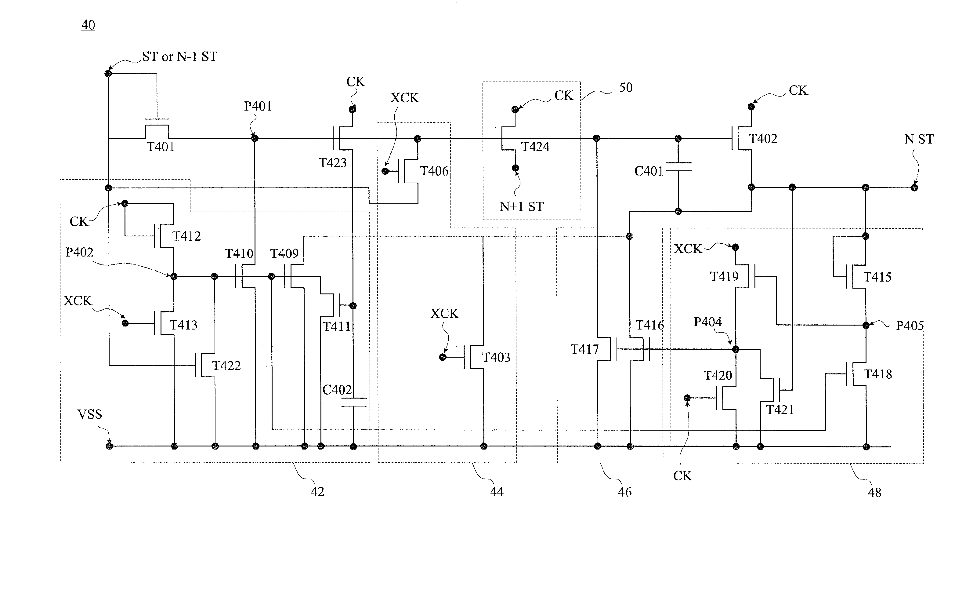
[0008]One objective of the present invention is to provide a single-stage shift register with individual driving node to prevent the abnormal operation of driving circuit due to a driving signal error in signal stage. Further, the complexity of a test procedure of the liquid crystal panel is effectively improved.
[0010]The shift register of the present invention utilizes a driving output unit for outputting a driving pulse signal to a shift register in next stage so that an incorrect driving signal of the shift register is avoided when the shift register has short circuit or signal error in previous stage. In addition, while performing a test procedure of the panel, the present invention is capable of locating the fault pixels on the panel. Therefore, the test correction of the pixels in next different stages can be completed to reduce the test complexity even though a fault pixel is located in the previous stage.

Problems solved by technology

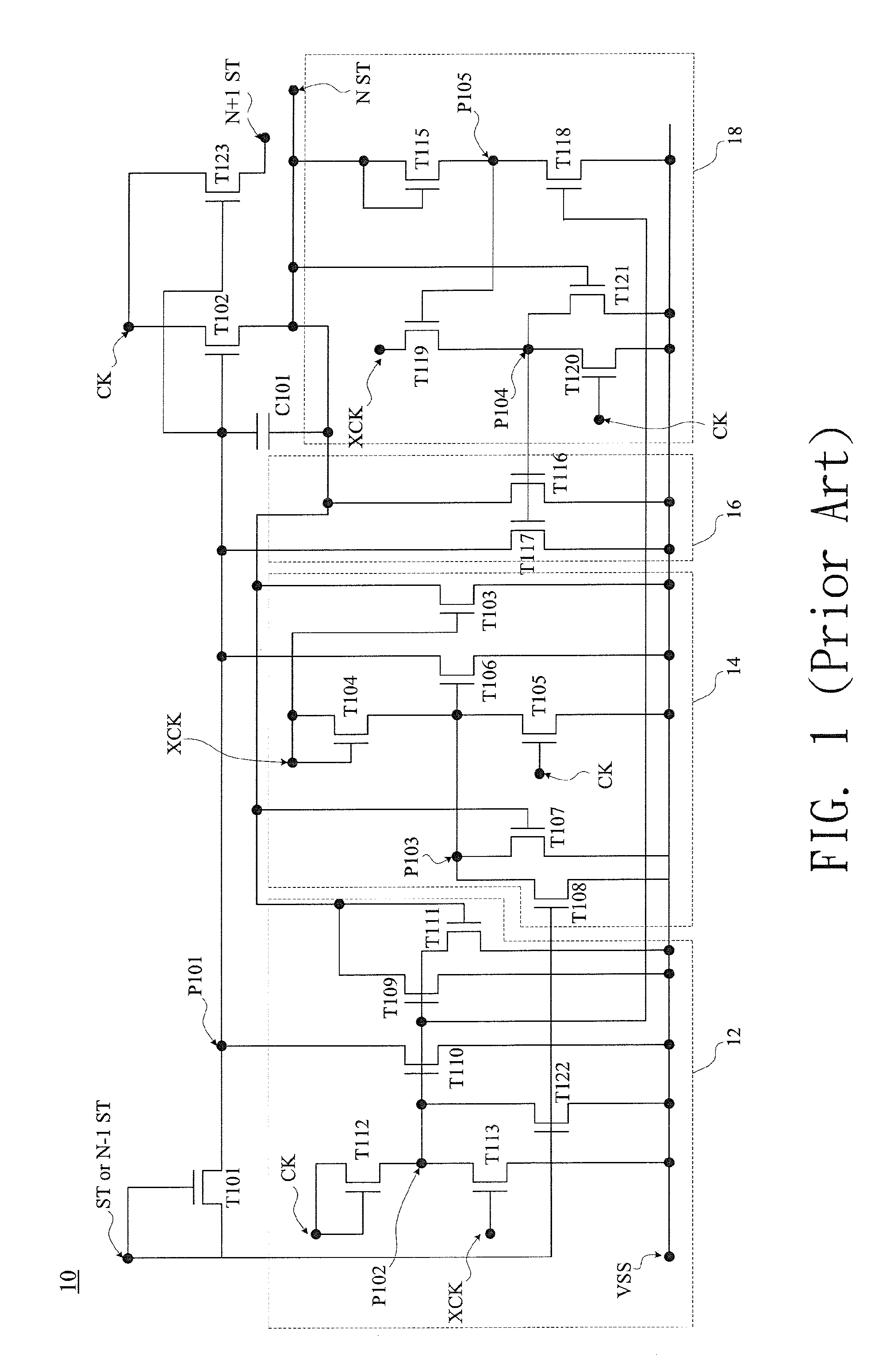
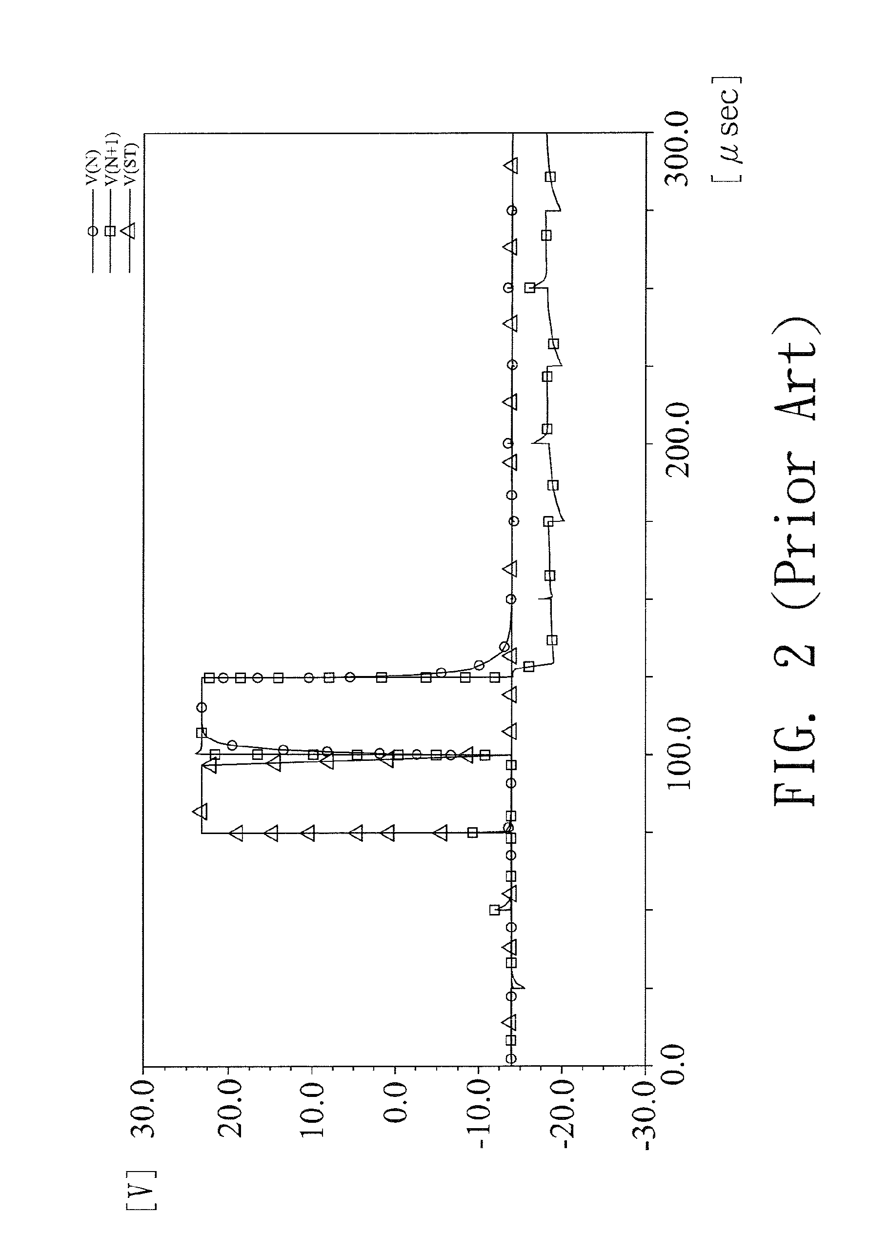
However, due to the circuit configuration of the conventional shift register, transistors “T102” and “T103” cannot be closed normally when the signal of outputting node “N” cannot be changed due to the short or signal errors happening to the pixels within the panel.
Thus, the waveform “V(N+1)” in the driving node “N+1 ST” has a jump and drops off to low voltage level so that the pixels in the stage (N+1) have errors and cannot operate correctly.
Such situation affects the operation of the driving circuit of the liquid crystal panel and further increase the complexity while performing a test procedure.

Method used


Image

  • Shift register with individual driving node
  • Shift register with individual driving node
  • Shift register with individual driving node

Examples


Embodiment Construction

[0016]FIG. 5 is a block diagram of a liquid crystal display 500 according to one embodiment of the present invention. The liquid crystal display 500 includes a liquid crystal panel 512, a gate driver 514, and a source driver 516. The liquid crystal panel 512 has a plurality of pixels and each pixel is composed of pixel unit 520 having three primary colors, i.e. red, green, and blue colors, respectively. The gate driver 514 outputs a scan signal so that each transistor 522 in each row is triggered sequentially. Meanwhile, the source driver 516 outputs corresponding data signal to the pixel units 520 in the row so that each pixel unit 520 are charged to display different gray-voltage level correctly. When the transistor 522 in a row are charged completely, the gate driver 514 closes the triggered row and outputs the scan signal for triggering the transistors 522 in the next row. Then, the source driver 516 outputs corresponding data signal for charging the pixel units 520 in the next ...


PUM


Abstract

A shift register having individual driving nodes is disclosed. The shift register includes a first clock pull-down module, a second clock pull-down module, a key pull-down module, a self feedback module, and a driving output unit. The first clock pull-down module is used to pull-down the potential of a gate line to a low voltage when the first clock signal is in a high voltage level. The second clock signal pull-down module pulls down the potential of the gate line to the low voltage when the second clock signal is in a high voltage level. The key pull-down module rapidly pulls down the potential of the gate line to the low voltage level after the gate line outputs an output signal. The self feedback module is used to output a driving signal to the key pull-down module. The driving signal output unit outputs a next stage driving signal which is irrelative to the operation of the previous stage shift register.

Description

FIELD OF THE INVENTION[0001]The present invention relates to a shift register, and more particularly to a single-stage shift register having individual driving node.BACKGROUND OF THE INVENTION[0002]The displays with advanced functions play an important role in consumer electronic products. Liquid crystal displays serve as the chromatic screens having high resolution, which are widely utilized in mobile phones, personal digital assistants (PDAs), digital still cameras, computer displays, and notebook displays. The shift register, an important electric component in the driving circuit of a liquid crystal display panel, is widely used to drive the display circuits of the liquid crystal display panel. As a result, the design of shift register is closely related to the characteristics of the liquid crystal display panel, such as power consumption and reliability.[0003]FIG. 1 is a conventional electric circuit of a single-stage shift register. The shift register 10 includes a “CK” clock p...

Claims


Application Information

Patent Timeline
Patent Type & Authority Patents(United States)
IPC IPC(8): G11C19/00
CPCG09G3/006G11C19/184G09G3/3674G09G2330/08
Inventor WEI, CHUN-CHINGLO, SHIH-HSUNYEH, YEN-HSIENCHIU, CHEN-LUNWU, YANG-EN
Owner AU OPTRONICS CORP
Why Eureka
Try Eureka